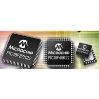
PIC18F46K22-I/MV Microchip Technology, PIC18F46K22-I/MV Datasheet - Page 40

PIC18F46K22-I/MV
Manufacturer Part Number
PIC18F46K22-I/MV
Description
64KB, Flash, 3968bytes-RAM,8-bit Family,nanoWatt XLP 40 UQFN 5x5x0.5mm TUBE
Manufacturer
Microchip Technology
Series
PIC® XLP™ 18Fr
Datasheet
1.PIC18F26J13-ISS.pdf
(496 pages)
Specifications of PIC18F46K22-I/MV
Core Processor
PIC
Core Size
8-Bit
Speed
64MHz
Connectivity
I²C, SPI, UART/USART
Peripherals
Brown-out Detect/Reset, HLVD, POR, PWM, WDT
Number Of I /o
35
Program Memory Size
64KB (32K x 16)
Program Memory Type
FLASH
Eeprom Size
1K x 8
Ram Size
3.8K x 8
Voltage - Supply (vcc/vdd)
1.8 V ~ 5.5 V
Data Converters
A/D 30x10b
Oscillator Type
Internal
Operating Temperature
-40°C ~ 85°C
Package / Case
40-UFQFN Exposed Pad
Processor Series
PIC18F
Core
PIC
Data Bus Width
8 bit
Data Ram Size
4 KB
Number Of Programmable I/os
36
Number Of Timers
3 x 8-bit. 4 x 16-bit
Operating Supply Voltage
1.8 V to 5.5 V
Mounting Style
SMD/SMT
Lead Free Status / RoHS Status
Lead free / RoHS Compliant
Lead Free Status / RoHS Status
Lead free / RoHS Compliant
- Current page: 40 of 496
- Download datasheet (5Mb)
PIC18(L)F2X/4XK22
2.7
For more information about the modes discussed in this
section see Section 3.0 “Power-Managed Modes”. A
quick reference list is also available in
When PRI_IDLE mode is selected, the designated
primary oscillator continues to run without interruption.
For all other power-managed modes, the oscillator
using the OSC1 pin is disabled. The OSC1 pin (and
OSC2 pin, if used by the oscillator) will stop oscillating.
In
SEC_IDLE), the secondary oscillator (SOSC) is
operating and providing the device clock. The
secondary oscillator may also run in all power-
managed modes if required to clock Timer1, Timer3 or
Timer5.
In internal oscillator modes (INTOSC_RUN and
INTOSC_IDLE), the internal oscillator block provides
the device clock source. The 31.25 kHz LFINTOSC
output can be used directly to provide the clock and
may be enabled to support various special features,
regardless
Section 24.2
Section 2.10 “Two-Speed Clock Start-up Mode”
Section 2.11 “Fail-Safe Clock Monitor”
information on WDT, Fail-Safe Clock Monitor and Two-
Speed Start-up). The HFINTOSC and MFINTOSC
outputs may be used directly to clock the device or may
be divided down by the postscaler. The HFINTOSC
and MFINTOSC outputs are disabled when the clock is
provided directly from the LFINTOSC output.
When the Sleep mode is selected, all clock sources are
stopped. Since all the transistor switching currents
have been stopped, Sleep mode achieves the lowest
current consumption of the device (only leakage
currents).
Enabling any on-chip feature that will operate during
Sleep will increase the current consumed during Sleep.
The LFINTOSC is required to support WDT operation.
Other features may be operating that do not require a
device clock source (i.e., SSP slave, PSP, INTn pins
and others). Peripherals that may add significant
current consumption are listed in
Characteristics:
PIC18(L)F2X/4XK22”.
DS41412D-page 40
secondary
Effects of Power-Managed Modes
on the Various Clock Sources
of
the
“Watchdog
clock
Input/Output
power-managed
modes
Timer
Section 27.8 “DC
(SEC_RUN
Characteristics,
Table
mode
3-1.
for more
(WDT)”,
(see
and
and
Preliminary
2.8
Power-up delays are controlled by two timers, so that
no external Reset circuitry is required for most
applications. The delays ensure that the device is kept
in Reset until the device power supply is stable under
normal circumstances and the primary clock is
operating and stable. For additional information on
power-up delays, see Section 4.5 “Device Reset
Timers”.
The first timer is the Power-up Timer (PWRT), which
provides a fixed delay on power-up. It is enabled by
clearing (= 0) the PWRTEN Configuration bit.
The second timer is the Oscillator Start-up Timer
(OST), intended to keep the chip in Reset until the
crystal oscillator is stable (LP, XT and HS modes). The
OST does this by counting 1024 oscillator cycles
before allowing the oscillator to clock the device.
When the PLL is enabled with external oscillator
modes, the device is kept in Reset for an additional
2 ms, following the OST delay, so the PLL can lock to
the incoming clock frequency.
There is a delay of interval T
the controller becomes ready to execute instructions.
This delay runs concurrently with any other delays.
This may be the only delay that occurs when any of the
EC, RC or INTIOSC modes are used as the primary
clock source.
When the HFINTOSC is selected as the primary clock,
the main system clock can be delayed until the
HFINTOSC is stable. This is user selectable by the
HFOFST bit of the CONFIG3H Configuration register.
When the HFOFST bit is cleared, the main system
clock is delayed until the HFINTOSC is stable. When
the HFOFST bit is set, the main system clock starts
immediately.
In either case, the HFIOFS bit of the OSCCON register
can be read to determine whether the HFINTOSC is
operating and stable.
Power-up Delays
2010 Microchip Technology Inc.
CSD
, following POR, while
Related parts for PIC18F46K22-I/MV
Image
Part Number
Description
Manufacturer
Datasheet
Request
R

Part Number:
Description:
Manufacturer:
Microchip Technology Inc.
Datasheet:

Part Number:
Description:
Manufacturer:
Microchip Technology Inc.
Datasheet:

Part Number:
Description:
Manufacturer:
Microchip Technology Inc.
Datasheet:

Part Number:
Description:
Manufacturer:
Microchip Technology Inc.
Datasheet:

Part Number:
Description:
Manufacturer:
Microchip Technology Inc.
Datasheet:

Part Number:
Description:
Manufacturer:
Microchip Technology Inc.
Datasheet:

Part Number:
Description:
Manufacturer:
Microchip Technology Inc.
Datasheet:

Part Number:
Description:
Manufacturer:
Microchip Technology Inc.
Datasheet:


