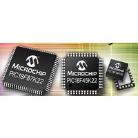
PIC18F46K22-I/MV Microchip Technology, PIC18F46K22-I/MV Datasheet - Page 355

PIC18F46K22-I/MV
Manufacturer Part Number
PIC18F46K22-I/MV
Description
64KB, Flash, 3968bytes-RAM,8-bit Family,nanoWatt XLP 40 UQFN 5x5x0.5mm TUBE
Manufacturer
Microchip Technology
Series
PIC® XLP™ 18Fr
Datasheet
1.PIC18F26J13-ISS.pdf
(496 pages)
Specifications of PIC18F46K22-I/MV
Core Processor
PIC
Core Size
8-Bit
Speed
64MHz
Connectivity
I²C, SPI, UART/USART
Peripherals
Brown-out Detect/Reset, HLVD, POR, PWM, WDT
Number Of I /o
35
Program Memory Size
64KB (32K x 16)
Program Memory Type
FLASH
Eeprom Size
1K x 8
Ram Size
3.8K x 8
Voltage - Supply (vcc/vdd)
1.8 V ~ 5.5 V
Data Converters
A/D 30x10b
Oscillator Type
Internal
Operating Temperature
-40°C ~ 85°C
Package / Case
40-UFQFN Exposed Pad
Processor Series
PIC18F
Core
PIC
Data Bus Width
8 bit
Data Ram Size
4 KB
Number Of Programmable I/os
36
Number Of Timers
3 x 8-bit. 4 x 16-bit
Operating Supply Voltage
1.8 V to 5.5 V
Mounting Style
SMD/SMT
Lead Free Status / RoHS Status
Lead free / RoHS Compliant
Lead Free Status / RoHS Status
Lead free / RoHS Compliant
- Current page: 355 of 496
- Download datasheet (5Mb)
REGISTER 24-5:
REGISTER 24-6:
2010 Microchip Technology Inc.
bit 7
Legend:
R = Readable bit
-n = Value when device is unprogrammed
bit 7
bit 6
bit 5-3
bit 2
bit 1
bit 0
Note 1:
bit 7
Legend:
R = Readable bit
-n = Value when device is unprogrammed
bit 7-4
bit 3
bit 2
bit 1
bit 0
Note 1:
DEBUG
R/P-1
U-0
—
2:
(2)
Can only be changed by a programmer in high-voltage programming mode.
The DEBUG bit is managed automatically by device development tools including debuggers and programmers. For
normal device operations, this bit should be maintained as a ‘1’.
Available on PIC18(L)FX5K22 and PIC18(L)FX6K22 devices.
DEBUG: Background Debugger Enable bit
1 = Background debugger disabled, RB6 and RB7 configured as general purpose I/O pins
0 = Background debugger enabled, RB6 and RB7 are dedicated to In-Circuit Debug
XINST: Extended Instruction Set Enable bit
1 = Instruction set extension and Indexed Addressing mode enabled
0 = Instruction set extension and Indexed Addressing mode disabled (Legacy mode)
Unimplemented: Read as ‘0’
LVP: Single-Supply ICSP Enable bit
1 = Single-Supply ICSP enabled
0 = Single-Supply ICSP disabled
Unimplemented: Read as ‘0’
STVREN: Stack Full/Underflow Reset Enable bit
1 = Stack full/underflow will cause Reset
0 = Stack full/underflow will not cause Reset
Unimplemented: Read as ‘0’
CP3: Code Protection bit
1 = Block 3 not code-protected
0 = Block 3 code-protected
CP2: Code Protection bit
1 = Block 2 not code-protected
0 = Block 2 code-protected
CP1: Code Protection bit
1 = Block 1 not code-protected
0 = Block 1 code-protected
CP0: Code Protection bit
1 = Block 0 not code-protected
0 = Block 0 code-protected
XINST
R/P-0
U-0
—
CONFIG4L: CONFIGURATION REGISTER 4 LOW
CONFIG5L: CONFIGURATION REGISTER 5 LOW
P = Programmable bit
U-0
U-0
—
—
(1)
(1)
U-0
U-0
Preliminary
—
—
(2)
U = Unimplemented bit, read as ‘0’
x = Bit is unknown
U = Unimplemented bit, read as ‘0’
C = Clearable only bit
CP3
R/C-1
U-0
—
PIC18(L)F2X/4XK22
(1)
CP2
R/C-1
LVP
R/P-1
(1)
(1)
R/C-1
CP1
U-0
—
DS41412D-page 355
STVREN
R/P-1
R/C-1
CP0
bit 0
bit 0
Related parts for PIC18F46K22-I/MV
Image
Part Number
Description
Manufacturer
Datasheet
Request
R

Part Number:
Description:
Manufacturer:
Microchip Technology Inc.
Datasheet:

Part Number:
Description:
Manufacturer:
Microchip Technology Inc.
Datasheet:

Part Number:
Description:
Manufacturer:
Microchip Technology Inc.
Datasheet:

Part Number:
Description:
Manufacturer:
Microchip Technology Inc.
Datasheet:

Part Number:
Description:
Manufacturer:
Microchip Technology Inc.
Datasheet:

Part Number:
Description:
Manufacturer:
Microchip Technology Inc.
Datasheet:

Part Number:
Description:
Manufacturer:
Microchip Technology Inc.
Datasheet:

Part Number:
Description:
Manufacturer:
Microchip Technology Inc.
Datasheet:


