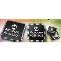
PIC18F46K22-I/MV Microchip Technology, PIC18F46K22-I/MV Datasheet - Page 181

PIC18F46K22-I/MV
Manufacturer Part Number
PIC18F46K22-I/MV
Description
64KB, Flash, 3968bytes-RAM,8-bit Family,nanoWatt XLP 40 UQFN 5x5x0.5mm TUBE
Manufacturer
Microchip Technology
Series
PIC® XLP™ 18Fr
Datasheet
1.PIC18F26J13-ISS.pdf
(496 pages)
Specifications of PIC18F46K22-I/MV
Core Processor
PIC
Core Size
8-Bit
Speed
64MHz
Connectivity
I²C, SPI, UART/USART
Peripherals
Brown-out Detect/Reset, HLVD, POR, PWM, WDT
Number Of I /o
35
Program Memory Size
64KB (32K x 16)
Program Memory Type
FLASH
Eeprom Size
1K x 8
Ram Size
3.8K x 8
Voltage - Supply (vcc/vdd)
1.8 V ~ 5.5 V
Data Converters
A/D 30x10b
Oscillator Type
Internal
Operating Temperature
-40°C ~ 85°C
Package / Case
40-UFQFN Exposed Pad
Processor Series
PIC18F
Core
PIC
Data Bus Width
8 bit
Data Ram Size
4 KB
Number Of Programmable I/os
36
Number Of Timers
3 x 8-bit. 4 x 16-bit
Operating Supply Voltage
1.8 V to 5.5 V
Mounting Style
SMD/SMT
Lead Free Status / RoHS Status
Lead free / RoHS Compliant
Lead Free Status / RoHS Status
Lead free / RoHS Compliant
- Current page: 181 of 496
- Download datasheet (5Mb)
14.2
The Compare mode function described in this section
is identical for all CCP and ECCP modules available on
this device family.
Compare mode makes use of the 16-bit TimerX
resources, Timer1, Timer3 and Timer5. The 16-bit
value of the CCPRxH:CCPRxL register pair is
constantly compared against the 16-bit value of the
TMRxH:TMRxL register pair. When a match occurs,
one of the following events can occur:
• Toggle the CCPx output
• Set the CCPx output
• Clear the CCPx output
• Generate a Special Event Trigger
• Generate a Software Interrupt
The action on the pin is based on the value of the
CCPxM<3:0> control bits of the CCPxCON register. At
the same time, the interrupt flag CCPxIF bit is set.
All Compare modes can generate an interrupt.
Figure 14-2
Compare operation.
FIGURE 14-2:
2010 Microchip Technology Inc.
Special Event Trigger function on
• ECCP1, ECCP2, ECCP3, CCP4 and CCP5 will:
Additional Function on
• CCP5 will
CCPx
Pin
- Reset TimerX – TMRxH:TMRxL = 0x0000
- TimerX Interrupt Flag, (TMRxIF) is not set
-
Output Enable
Conversion if ADCON<0>, ADON = 1.
Set ADCON0<1>, GO/DONE bit to start an ADC
TRIS
Compare Mode
shows a simplified diagram of the
Q
Special Event Trigger
CCPxM<3:0>
R
S
Mode Select
Output
COMPARE MODE
OPERATION BLOCK
DIAGRAM
Logic
Set CCPxIF Interrupt Flag
4
(PIR1/2/4)
Match
CCPRxH CCPRxL
TMRxH
Comparator
TMRxL
Preliminary
14.2.1
The user must configure the CCPx pin as an output by
clearing the associated TRIS bit.
Some CCPx outputs are multiplexed on a couple of
pins.
Multiplexing. Selection of the output pin is determined
by the CCPxMX bits in Configuration register 3H
(CONFIG3H). Refer to
14.2.2
In Compare mode, 16-bit TimerX resource must be
running in either Timer mode or Synchronized Counter
mode. The compare operation may not work in
Asynchronous Counter mode.
See
Control”
TimerX resources.
14.2.3
When Generate Software Interrupt mode is chosen
(CCPxM<3:0> = 1010), the CCPx module does not
assert control of the CCPx pin (see the CCPxCON
register).
Note:
Note:
PIC18(L)F2X/4XK22
Section 12.0 “Timer1/3/5 Module with Gate
Table 14-2
for more information on configuring the 16-bit
CCP PIN CONFIGURATION
Clearing the CCPxCON register will force
the CCPx compare output latch to the
default low level. This is not the PORT I/O
data latch.
TimerX MODE RESOURCE
Clocking TimerX from the system clock
(F
mode. In order for Compare mode to
recognize the trigger event on the CCPx
pin, TimerX must be clocked from the
instruction clock (F
external clock source.
SOFTWARE INTERRUPT MODE
OSC
) should not be used in Compare
shows
Register 24-4
the
OSC
CCP
DS41412D-page 181
/4) or from an
for more details.
output
pin
Related parts for PIC18F46K22-I/MV
Image
Part Number
Description
Manufacturer
Datasheet
Request
R

Part Number:
Description:
Manufacturer:
Microchip Technology Inc.
Datasheet:

Part Number:
Description:
Manufacturer:
Microchip Technology Inc.
Datasheet:

Part Number:
Description:
Manufacturer:
Microchip Technology Inc.
Datasheet:

Part Number:
Description:
Manufacturer:
Microchip Technology Inc.
Datasheet:

Part Number:
Description:
Manufacturer:
Microchip Technology Inc.
Datasheet:

Part Number:
Description:
Manufacturer:
Microchip Technology Inc.
Datasheet:

Part Number:
Description:
Manufacturer:
Microchip Technology Inc.
Datasheet:

Part Number:
Description:
Manufacturer:
Microchip Technology Inc.
Datasheet:


