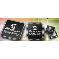
PIC18F46K22-I/MV Microchip Technology, PIC18F46K22-I/MV Datasheet - Page 182

PIC18F46K22-I/MV
Manufacturer Part Number
PIC18F46K22-I/MV
Description
64KB, Flash, 3968bytes-RAM,8-bit Family,nanoWatt XLP 40 UQFN 5x5x0.5mm TUBE
Manufacturer
Microchip Technology
Series
PIC® XLP™ 18Fr
Datasheet
1.PIC18F26J13-ISS.pdf
(496 pages)
Specifications of PIC18F46K22-I/MV
Core Processor
PIC
Core Size
8-Bit
Speed
64MHz
Connectivity
I²C, SPI, UART/USART
Peripherals
Brown-out Detect/Reset, HLVD, POR, PWM, WDT
Number Of I /o
35
Program Memory Size
64KB (32K x 16)
Program Memory Type
FLASH
Eeprom Size
1K x 8
Ram Size
3.8K x 8
Voltage - Supply (vcc/vdd)
1.8 V ~ 5.5 V
Data Converters
A/D 30x10b
Oscillator Type
Internal
Operating Temperature
-40°C ~ 85°C
Package / Case
40-UFQFN Exposed Pad
Processor Series
PIC18F
Core
PIC
Data Bus Width
8 bit
Data Ram Size
4 KB
Number Of Programmable I/os
36
Number Of Timers
3 x 8-bit. 4 x 16-bit
Operating Supply Voltage
1.8 V to 5.5 V
Mounting Style
SMD/SMT
Lead Free Status / RoHS Status
Lead free / RoHS Compliant
Lead Free Status / RoHS Status
Lead free / RoHS Compliant
- Current page: 182 of 496
- Download datasheet (5Mb)
PIC18(L)F2X/4XK22
14.2.4
When Special Event Trigger mode is selected
(CCPxM<3:0> = 1011),
TMRxH:TMRxL and the CCPRxH:CCPRxL registers
occurs, all CCPx and ECCPx modules will immediately:
• Set the CCP interrupt flag bit – CCPxIF
• CCP5 will start an ADC conversion, if the ADC is
On the next TimerX rising clock edge:
• A Reset of TimerX register pair occurs –
This Special Event Trigger mode does not:
• Assert control over the CCPx or ECCPx pins.
• Set the TMRxIF interrupt bit when the
If the value of the CCPRxH:CCPRxL registers are
modified when a match occurs, the user should be
aware that the automatic reset of TimerX occurs on the
next rising edge of the clock. Therefore, modifying the
CCPRxH:CCPRxL registers before this reset occurs
will allow the TimerX to continue without being reset,
inadvertently resulting in the next event being
advanced or delayed.
The
CCPRxH:CCPRxL register pair to effectively provide a
16-bit programmable period register for TimerX.
TABLE 14-5:
DS41412D-page 182
CCP1CON
CCP2CON
CCP3CON
CCP4CON
CCP5CON
CCPR1H
CCPR1L
CCPR2H
CCPR2L
CCPR3H
CCPR3L
CCPR4H
CCPR4L
CCPR5H
CCPR5L
CCPTMRS0
CCPTMRS1
INTCON
Legend: — = Unimplemented location, read as ‘0’. Shaded bits are not used by Capture mode.
Note
enabled
TMRxH:TMRxL = 0x0000,
TMRxH:TMRxL register pair is reset. (TMRxIF
gets set on a TimerX overflow.)
Name
Special
1:
These registers/bits are available on PIC18(L)F4XK22 devices.
SPECIAL EVENT TRIGGER
GIE/GIEH
Event
Bit 7
REGISTERS ASSOCIATED WITH COMPARE
—
—
—
C3TSEL<1:0>
P1M<1:0>
P2M<1:0>
P3M<1:0>
Trigger
and
PEIE/GIEL
Bit 6
—
—
—
a
mode
match
Capture/Compare/PWM Register 1 High Byte (MSB)
Capture/Compare/PWM Register 2 High Byte (MSB)
Capture/Compare/PWM Register 3 High Byte (MSB)
Capture/Compare/PWM Register 4 High Byte (MSB)
Capture/Compare/PWM Register 5 High Byte (MSB)
Capture/Compare/PWM Register 1 Low Byte (LSB)
Capture/Compare/PWM Register 2 Low Byte (LSB)
Capture/Compare/PWM Register 3 Low Byte (LSB)
Capture/Compare/PWM Register 4 Low Byte (LSB)
Capture/Compare/PWM Register 5 Low Byte (LSB)
TMR0IE
Bit 5
allows
—
—
DC1B<1:0>
DC2B<1:0>
DC3B<1:0>
DC4B<1:0>
DC5B<1:0>
of
Preliminary
the
the
INT0IE
Bit 4
—
C2TSEL<1:0>
14.2.5
The Compare mode is dependent upon the system
clock (F
down during Sleep mode, the Compare mode will not
function properly during Sleep.
RBIE
Bit 3
C5TSEL<1:0>
OSC
COMPARE DURING SLEEP
) for proper operation. Since F
TMR0IF
Bit 2
CCP1M<3:0>
CCP2M<3:0>
CCP3M<3:0>
CCP4M<3:0>
CCP5M<3:0>
—
2010 Microchip Technology Inc.
INT0IF
Bit 1
C1TSEL<1:0>
C4TSEL<1:0>
RBIF
Bit 0
OSC
Register
on Page
is shut
201
201
201
201
201
204
204
115
—
—
—
—
—
—
—
—
—
—
Related parts for PIC18F46K22-I/MV
Image
Part Number
Description
Manufacturer
Datasheet
Request
R

Part Number:
Description:
Manufacturer:
Microchip Technology Inc.
Datasheet:

Part Number:
Description:
Manufacturer:
Microchip Technology Inc.
Datasheet:

Part Number:
Description:
Manufacturer:
Microchip Technology Inc.
Datasheet:

Part Number:
Description:
Manufacturer:
Microchip Technology Inc.
Datasheet:

Part Number:
Description:
Manufacturer:
Microchip Technology Inc.
Datasheet:

Part Number:
Description:
Manufacturer:
Microchip Technology Inc.
Datasheet:

Part Number:
Description:
Manufacturer:
Microchip Technology Inc.
Datasheet:

Part Number:
Description:
Manufacturer:
Microchip Technology Inc.
Datasheet:


