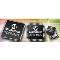
PIC18F46K22-I/MV Microchip Technology, PIC18F46K22-I/MV Datasheet - Page 17

PIC18F46K22-I/MV
Manufacturer Part Number
PIC18F46K22-I/MV
Description
64KB, Flash, 3968bytes-RAM,8-bit Family,nanoWatt XLP 40 UQFN 5x5x0.5mm TUBE
Manufacturer
Microchip Technology
Series
PIC® XLP™ 18Fr
Datasheet
1.PIC18F26J13-ISS.pdf
(496 pages)
Specifications of PIC18F46K22-I/MV
Core Processor
PIC
Core Size
8-Bit
Speed
64MHz
Connectivity
I²C, SPI, UART/USART
Peripherals
Brown-out Detect/Reset, HLVD, POR, PWM, WDT
Number Of I /o
35
Program Memory Size
64KB (32K x 16)
Program Memory Type
FLASH
Eeprom Size
1K x 8
Ram Size
3.8K x 8
Voltage - Supply (vcc/vdd)
1.8 V ~ 5.5 V
Data Converters
A/D 30x10b
Oscillator Type
Internal
Operating Temperature
-40°C ~ 85°C
Package / Case
40-UFQFN Exposed Pad
Processor Series
PIC18F
Core
PIC
Data Bus Width
8 bit
Data Ram Size
4 KB
Number Of Programmable I/os
36
Number Of Timers
3 x 8-bit. 4 x 16-bit
Operating Supply Voltage
1.8 V to 5.5 V
Mounting Style
SMD/SMT
Lead Free Status / RoHS Status
Lead free / RoHS Compliant
Lead Free Status / RoHS Status
Lead free / RoHS Compliant
- Current page: 17 of 496
- Download datasheet (5Mb)
TABLE 1-2:
2010 Microchip Technology Inc.
Legend:
Note 1:
PDIP,
SOIC
Pin Number
10
2
3
4
5
6
7
2:
UQFN
QFN,
27
28
TTL = TTL compatible input CMOS = CMOS compatible input or output; ST = Schmitt Trigger input with CMOS levels;
I = Input; O = Output; P = Power.
Default pin assignment for P2B, T3CKI, CCP3 and CCP2 when Configuration bits PB2MX, T3CMX, CCP3MX and
CCP2MX are set.
Alternate pin assignment for P2B, T3CKI, CCP3 and CCP2 when Configuration bits PB2MX, T3CMX, CCP3MX and
CCP2MX are clear.
1
2
3
4
7
RA0/C12IN0-/AN0
RA1/C12IN1-/AN1
RA2/C2IN+/AN2/DACOUT/V
RA3/C1IN+/AN3/V
RA4/CCP5/C1OUT/SRQ/T0CKI
RA5/C2OUT/SRNQ/SS1/HLVDIN/AN4
RA6/CLKO/OSC2
PIC18(L)F2XK22 PINOUT I/O DESCRIPTIONS
Pin Name
DACOUT
C12IN0-
C12IN1-
HLVDIN
C1OUT
C2OUT
C2IN+
C1IN+
T0CKI
SRNQ
V
CLKO
OSC2
V
CCP5
SRQ
RA0
AN0
RA1
AN1
RA2
AN2
RA3
AN3
RA4
RA5
AN4
RA6
SS1
REF
REF
REF
+
-
+
REF
-
Preliminary
Type
Pin
I/O
I/O
I/O
I/O
I/O
I/O
I/O
I/O
O
O
O
O
O
O
O
I
I
I
I
I
I
I
I
I
I
I
I
I
I
Analog Comparators C1 and C2 inverting input.
Analog Analog input 0.
Analog Comparators C1 and C2 inverting input.
Analog Analog input 1.
Analog Comparator C2 non-inverting input.
Analog Analog input 2.
Analog DAC Reference output.
Analog A/D reference voltage (low) input.
Analog Comparator C1 non-inverting input.
Analog Analog input 3.
Analog A/D reference voltage (high) input.
Analog High/Low-Voltage Detect input.
Analog Analog input 4.
Buffer
CMOS
CMOS
Type
TTL
TTL
TTL
TTL
TTL
TTL
TTL
TTL
TTL
ST
ST
ST
PIC18(L)F2X/4XK22
Digital I/O.
Digital I/O.
Digital I/O.
Digital I/O.
Digital I/O.
Capture 5 input/Compare 5 output/PWM 5 output.
Comparator C1 output.
SR Latch Q output.
Timer0 external clock input.
Digital I/O.
Comparator C2 output.
SR Latch Q output.
SPI slave select input (MSSP1).
Digital I/O.
In RC mode, OSC2 pin outputs CLKOUT which has
1/4 the frequency of OSC1 and denotes the instruction
cycle rate.
Oscillator crystal output. Connects to crystal or resonator
in Crystal Oscillator mode.
Description
DS41412D-page 17
Related parts for PIC18F46K22-I/MV
Image
Part Number
Description
Manufacturer
Datasheet
Request
R

Part Number:
Description:
Manufacturer:
Microchip Technology Inc.
Datasheet:

Part Number:
Description:
Manufacturer:
Microchip Technology Inc.
Datasheet:

Part Number:
Description:
Manufacturer:
Microchip Technology Inc.
Datasheet:

Part Number:
Description:
Manufacturer:
Microchip Technology Inc.
Datasheet:

Part Number:
Description:
Manufacturer:
Microchip Technology Inc.
Datasheet:

Part Number:
Description:
Manufacturer:
Microchip Technology Inc.
Datasheet:

Part Number:
Description:
Manufacturer:
Microchip Technology Inc.
Datasheet:

Part Number:
Description:
Manufacturer:
Microchip Technology Inc.
Datasheet:


