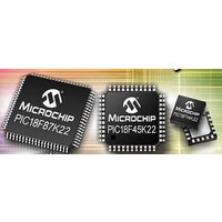
PIC18F46K22-I/MV Microchip Technology, PIC18F46K22-I/MV Datasheet - Page 201

PIC18F46K22-I/MV
Manufacturer Part Number
PIC18F46K22-I/MV
Description
64KB, Flash, 3968bytes-RAM,8-bit Family,nanoWatt XLP 40 UQFN 5x5x0.5mm TUBE
Manufacturer
Microchip Technology
Series
PIC® XLP™ 18Fr
Datasheet
1.PIC18F26J13-ISS.pdf
(496 pages)
Specifications of PIC18F46K22-I/MV
Core Processor
PIC
Core Size
8-Bit
Speed
64MHz
Connectivity
I²C, SPI, UART/USART
Peripherals
Brown-out Detect/Reset, HLVD, POR, PWM, WDT
Number Of I /o
35
Program Memory Size
64KB (32K x 16)
Program Memory Type
FLASH
Eeprom Size
1K x 8
Ram Size
3.8K x 8
Voltage - Supply (vcc/vdd)
1.8 V ~ 5.5 V
Data Converters
A/D 30x10b
Oscillator Type
Internal
Operating Temperature
-40°C ~ 85°C
Package / Case
40-UFQFN Exposed Pad
Processor Series
PIC18F
Core
PIC
Data Bus Width
8 bit
Data Ram Size
4 KB
Number Of Programmable I/os
36
Number Of Timers
3 x 8-bit. 4 x 16-bit
Operating Supply Voltage
1.8 V to 5.5 V
Mounting Style
SMD/SMT
Lead Free Status / RoHS Status
Lead free / RoHS Compliant
Lead Free Status / RoHS Status
Lead free / RoHS Compliant
- Current page: 201 of 496
- Download datasheet (5Mb)
TABLE 14-14: CONFIGURATION REGISTERS ASSOCIATED WITH CAPTURE
REGISTER 14-1:
2010 Microchip Technology Inc.
CONFIG3H
Legend: — = Unimplemented location, read as ‘0’. Shaded bits are not used by Capture mode.
bit 7
Legend:
R = Readable bit
u = Bit is unchanged
‘1’ = Bit is set
bit 7-6
bit 5-4
bit 3-0
Note 1:
Name
U-0
—
This feature is available on CCP5 only.
MCLRE
Bit 7
Unused
DCxB<1:0>: PWM Duty Cycle Least Significant bits
Capture mode:
Unused
Compare mode:
Unused
PWM mode:
These bits are the two LSbs of the PWM duty cycle. The eight MSbs are found in CCPRxL.
CCPxM<3:0>: ECCPx Mode Select bits
0000 = Capture/Compare/PWM off (resets the module)
0001 = Reserved
0010 = Compare mode: toggle output on match
0011 = Reserved
0100 = Capture mode: every falling edge
0101 = Capture mode: every rising edge
0110 = Capture mode: every 4th rising edge
0111 = Capture mode: every 16th rising edge
1000 = Compare mode: set output on compare match (CCPx pin is set, CCPxIF is set)
1001 = Compare mode: clear output on compare match (CCPx pin is cleared, CCPxIF is set)
1010 = Compare mode: generate software interrupt on compare match (CCPx pin is unaffected,
1011 = Compare mode: Special Event Trigger (CCPx pin is unaffected, CCPxIF is set)
11xx =: PWM mode
U-0
—
CCPxCON: STANDARD CCPx CONTROL REGISTER
CCPxIF is set)
Bit 6
—
W = Writable bit
x = Bit is unknown
‘0’ = Bit is cleared
R/W-0
P2BMX
Bit 5
DCxB<1:0>
TimerX (selected by CxTSEL bits) is reset
ADON is set, starting A/D conversion if A/D module is enabled
T3CMX
R/W-0
Bit 4
Preliminary
HFOFST
U = Unimplemented bit, read as ‘0’
-n/n = Value at POR and BOR/Value at all other Reset
Bit 3
R/W-0
PIC18(L)F2X/4XK22
CCP3MX
Bit 2
R/W-0
CCPxM<3:0>
PBADEN
Bit 1
R/W-0
CCP2MX
DS41412D-page 201
Bit 0
(1)
R/W-0
Register
on Page
354
bit 0
Related parts for PIC18F46K22-I/MV
Image
Part Number
Description
Manufacturer
Datasheet
Request
R

Part Number:
Description:
Manufacturer:
Microchip Technology Inc.
Datasheet:

Part Number:
Description:
Manufacturer:
Microchip Technology Inc.
Datasheet:

Part Number:
Description:
Manufacturer:
Microchip Technology Inc.
Datasheet:

Part Number:
Description:
Manufacturer:
Microchip Technology Inc.
Datasheet:

Part Number:
Description:
Manufacturer:
Microchip Technology Inc.
Datasheet:

Part Number:
Description:
Manufacturer:
Microchip Technology Inc.
Datasheet:

Part Number:
Description:
Manufacturer:
Microchip Technology Inc.
Datasheet:

Part Number:
Description:
Manufacturer:
Microchip Technology Inc.
Datasheet:


