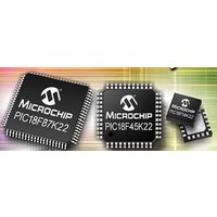
PIC18F46K22-I/MV Microchip Technology, PIC18F46K22-I/MV Datasheet - Page 56

PIC18F46K22-I/MV
Manufacturer Part Number
PIC18F46K22-I/MV
Description
64KB, Flash, 3968bytes-RAM,8-bit Family,nanoWatt XLP 40 UQFN 5x5x0.5mm TUBE
Manufacturer
Microchip Technology
Series
PIC® XLP™ 18Fr
Datasheet
1.PIC18F26J13-ISS.pdf
(496 pages)
Specifications of PIC18F46K22-I/MV
Core Processor
PIC
Core Size
8-Bit
Speed
64MHz
Connectivity
I²C, SPI, UART/USART
Peripherals
Brown-out Detect/Reset, HLVD, POR, PWM, WDT
Number Of I /o
35
Program Memory Size
64KB (32K x 16)
Program Memory Type
FLASH
Eeprom Size
1K x 8
Ram Size
3.8K x 8
Voltage - Supply (vcc/vdd)
1.8 V ~ 5.5 V
Data Converters
A/D 30x10b
Oscillator Type
Internal
Operating Temperature
-40°C ~ 85°C
Package / Case
40-UFQFN Exposed Pad
Processor Series
PIC18F
Core
PIC
Data Bus Width
8 bit
Data Ram Size
4 KB
Number Of Programmable I/os
36
Number Of Timers
3 x 8-bit. 4 x 16-bit
Operating Supply Voltage
1.8 V to 5.5 V
Mounting Style
SMD/SMT
Lead Free Status / RoHS Status
Lead free / RoHS Compliant
Lead Free Status / RoHS Status
Lead free / RoHS Compliant
- Current page: 56 of 496
- Download datasheet (5Mb)
PIC18(L)F2X/4XK22
3.6
Idle mode allows users to substantially reduce power
consumption by stopping the CPU clock. Even so,
peripheral modules still remain clocked, and thus, con-
sume power. There may be cases where the applica-
tion needs what IDLE mode does not provide: the
allocation of power resources to the CPU processing
with minimal power consumption from the peripherals.
PIC18(L)F2X/4XK22 family devices address this
requirement by allowing peripheral modules to be
selectively disabled, reducing or eliminating their
power consumption. This can be done with control bits
in the Peripheral Module Disable (PMD) registers.
These bits generically named XXXMD are located in
control registers PMD0, PMD1 or PMD2.
REGISTER 3-1:
DS41412D-page 56
bit 7
Legend:
R = Readable bit
-n = Value at POR
bit 7
bit 6
bit 5
bit 4
bit 3
bit 2
bit 1
bit 0
UART2MD
R/W-0
Selective Peripheral Module
Control
UART2MD: UART2 Peripheral Module Disable Control bit
1 = Module is disabled, Clock Source is disconnected, module does not draw digital power
0 = Module is enabled, Clock Source is connected, module draws digital power
UART1MD: UART1 Peripheral Module Disable Control bit
1 = Module is disabled, Clock Source is disconnected, module does not draw digital power
0 = Module is enabled, Clock Source is connected, module draws digital power
TMR6MD: Timer6 Peripheral Module Disable Control bit
1 = Module is disabled, Clock Source is disconnected, module does not draw digital power
0 = Module is enabled, Clock Source is connected, module draws digital power
TMR5MD: Timer5 Peripheral Module Disable Control bit
1 = Module is disabled, Clock Source is disconnected, module does not draw digital power
0 = Module is enabled, Clock Source is connected, module draws digital power
TMR4MD: Timer4 Peripheral Module Disable Control bit
1 = Module is disabled, Clock Source is disconnected, module does not draw digital power
0 = Module is enabled, Clock Source is connected, module draws digital power
TMR3MD: Timer3 Peripheral Module Disable Control bit
1 = Module is disabled, Clock Source is disconnected, module does not draw digital power
0 = Module is enabled, Clock Source is connected, module draws digital power
TMR2MD: Timer2 Peripheral Module Disable Control bit
1 = Module is disabled, Clock Source is disconnected, module does not draw digital power
0 = Module is enabled, Clock Source is connected, module draws digital power
TMR1MD: Timer1 Peripheral Module Disable Control bit
1 = Module is disabled, Clock Source is disconnected, module does not draw digital power
0 = Module is enabled, Clock Source is connected, module draws digital power
UART1MD
R/W-0
PMD0: PERIPHERAL MODULE DISABLE REGISTER 0
W = Writable bit
‘1’ = Bit is set
TMR6MD
R/W-0
TMR5MD
R/W-0
Preliminary
U = Unimplemented bit, read as ‘0’
‘0’ = Bit is cleared
TMR4MD
R/W-0
Setting the PMD bit for a module disables all clock
sources
consumption to an absolute minimum. In this state, the
control and STATUS registers associated with the
peripheral are also disabled, so writes to these
registers have no effect and read values are invalid.
to
TMR3MD
R/W-0
that
module,
2010 Microchip Technology Inc.
x = Bit is unknown
TMR2MD
R/W-0
reducing
TMR1MD
its
R/W-0
power
bit 0
Related parts for PIC18F46K22-I/MV
Image
Part Number
Description
Manufacturer
Datasheet
Request
R

Part Number:
Description:
Manufacturer:
Microchip Technology Inc.
Datasheet:

Part Number:
Description:
Manufacturer:
Microchip Technology Inc.
Datasheet:

Part Number:
Description:
Manufacturer:
Microchip Technology Inc.
Datasheet:

Part Number:
Description:
Manufacturer:
Microchip Technology Inc.
Datasheet:

Part Number:
Description:
Manufacturer:
Microchip Technology Inc.
Datasheet:

Part Number:
Description:
Manufacturer:
Microchip Technology Inc.
Datasheet:

Part Number:
Description:
Manufacturer:
Microchip Technology Inc.
Datasheet:

Part Number:
Description:
Manufacturer:
Microchip Technology Inc.
Datasheet:


