EVB9S12XEP100 Freescale Semiconductor, EVB9S12XEP100 Datasheet - Page 1221
EVB9S12XEP100
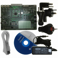
Manufacturer Part Number
EVB9S12XEP100
Description
BOARD EVAL FOR MC9S12XEP100
Manufacturer
Freescale Semiconductor
Type
MCUr
Datasheet
1.EVB9S12XEP100.pdf
(1328 pages)
Specifications of EVB9S12XEP100
Contents
Module and Misc Hardware
Processor To Be Evaluated
MC9S12XEP100
Data Bus Width
16 bit
Interface Type
RS-232
Silicon Manufacturer
Freescale
Core Architecture
S12
Core Sub-architecture
S12
Silicon Core Number
MC9S12
Silicon Family Name
S12XE
Rohs Compliant
Yes
For Use With/related Products
MC9S12XEP100
Lead Free Status / RoHS Status
Lead free / RoHS Compliant


A.2
This section describes the characteristics of the analog-to-digital converter.
A.2.1
The
The following constraints exist to obtain full-scale, full range results:
This constraint exists since the sample buffer amplifier can not drive beyond the power supply levels that
it ties to. If the input level goes outside of this range it will effectively be clipped.
1
2
3
A.2.2
Source resistance, source capacitance and current injection have an influence on the accuracy of the ATD.
A further factor is that PortAD pins that are configured as output drivers switching.
Freescale Semiconductor
Conditions are shown in
Num C
Full accuracy is not guaranteed when differential voltage is less than 4.50 V
When converting in Stop Mode (ICLKSTP=1) an ATD Stop Recovery time tATDSTPRCV is required to switch back to bus clock
based ATDCLK when leaving Stop Mode. Do not access ATD registers during this time.
The minimum time assumes a sample time of 4 ATD clock cycles. The maximum time assumes a sample time of 24 ATD clock
cycles and the discharge feature (SMP_DIS) enabled, which adds 2 ATD clock cycles.
1
2
3
4
5
6
7
8
Table A-15
D Reference potential
D Voltage difference V
D Voltage difference V
C Differential reference voltage
C ATD Clock Frequency (derived from bus clock via the
P ATD Clock Frequency in Stop mode (internal generated
D ADC conversion in stop, recovery time
D
V
SSA
prescaler)
temperature and voltage dependent clock, ICLK)
ATD Conversion Period
12 bit resolution:
10 bit resolution:
8 bit resolution:
ATD Characteristics
ATD Operating Characteristics
Factors Influencing Accuracy
Low
High
≤ V
and
RL
≤ V
Table A-16
Table A-4
IN
DDX
SSX
≤ V
3
unless otherwise noted, supply voltage 3.13V < V
to V
to V
Rating
RH
MC9S12XE-Family Reference Manual Rev. 1.23
Table A-15. ATD Operating Characteristics
show conditions under which the ATD operates.
SSA
DDA
1
≤ V
DDA
2
.
t
N
N
ATDSTPRC
N
V
Symbol
f
∆
∆
CONV12
CONV10
ATDCLk
RH
CONV8
V
V
VDDX
VSSX
RH
V
RL
-V
RL
V
–2.35
DDA
V
–0.1
3.13
0.25
DDA
Min
0.6
20
19
17
—
SSA
/2
< 5.5 V
Appendix A Electrical Characteristics
Typ
5.0
—
—
—
—
—
—
—
0
0
1
V
V
Max
DDA
0.1
0.1
5.5
8.3
1.7
1.5
42
41
39
DDA
/2
Cycles
clock
MHz
MHz
ATD
Unit
us
V
V
V
V
V
1221
Related parts for EVB9S12XEP100
Image
Part Number
Description
Manufacturer
Datasheet
Request
R

Part Number:
Description:
Manufacturer:
Freescale Semiconductor, Inc
Datasheet:
Part Number:
Description:
Manufacturer:
Freescale Semiconductor, Inc
Datasheet:
Part Number:
Description:
Manufacturer:
Freescale Semiconductor, Inc
Datasheet:
Part Number:
Description:
Manufacturer:
Freescale Semiconductor, Inc
Datasheet:
Part Number:
Description:
Manufacturer:
Freescale Semiconductor, Inc
Datasheet:
Part Number:
Description:
Manufacturer:
Freescale Semiconductor, Inc
Datasheet:
Part Number:
Description:
Manufacturer:
Freescale Semiconductor, Inc
Datasheet:
Part Number:
Description:
Manufacturer:
Freescale Semiconductor, Inc
Datasheet:
Part Number:
Description:
Manufacturer:
Freescale Semiconductor, Inc
Datasheet:
Part Number:
Description:
Manufacturer:
Freescale Semiconductor, Inc
Datasheet:
Part Number:
Description:
Manufacturer:
Freescale Semiconductor, Inc
Datasheet:
Part Number:
Description:
Manufacturer:
Freescale Semiconductor, Inc
Datasheet:
Part Number:
Description:
Manufacturer:
Freescale Semiconductor, Inc
Datasheet:
Part Number:
Description:
Manufacturer:
Freescale Semiconductor, Inc
Datasheet:
Part Number:
Description:
Manufacturer:
Freescale Semiconductor, Inc
Datasheet: