EVB9S12XEP100 Freescale Semiconductor, EVB9S12XEP100 Datasheet - Page 36
EVB9S12XEP100
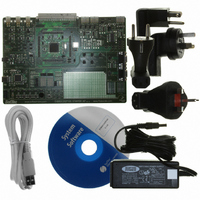
Manufacturer Part Number
EVB9S12XEP100
Description
BOARD EVAL FOR MC9S12XEP100
Manufacturer
Freescale Semiconductor
Type
MCUr
Datasheet
1.EVB9S12XEP100.pdf
(1328 pages)
Specifications of EVB9S12XEP100
Contents
Module and Misc Hardware
Processor To Be Evaluated
MC9S12XEP100
Data Bus Width
16 bit
Interface Type
RS-232
Silicon Manufacturer
Freescale
Core Architecture
S12
Core Sub-architecture
S12
Silicon Core Number
MC9S12
Silicon Family Name
S12XE
Rohs Compliant
Yes
For Use With/related Products
MC9S12XEP100
Lead Free Status / RoHS Status
Lead free / RoHS Compliant


Chapter 1 Device Overview MC9S12XE-Family
Unimplemented RAM pages are mapped externally in expanded modes. Accessing unimplemented RAM
pages in single chip modes causes an illegal address reset if the MPU is not configured to flag an MPU
protection error in that range.
Accessing unimplemented FLASH pages in single chip modes causes an illegal address reset if the MPU
is not configured to flag an MPU protection error in that range.
The PARTID value should be referenced regarding the specific memory map for any given device. For
devices sharing the same part ID, the memory regions which are implemented on the larger device but not
supported on the smaller device are implemented but untested on that smaller device. These regions do not
appear as unimplemented in the memory map and do not result in an illegal address reset if erroneously
accessed.
From the above the following examples can be derived.
The 9S12XEP768 is currently only available as a 9S12XEP100 die, thus the unimplemented FLASH pages
are those of the 9S12XEP100 device map.
The 9S12XEQ384, 9S12XEG384, 9S12XES384 are currently only available as a 9S12XEQ512 die, thus
the unimplemented FLASH pages are those of the 9S12XEQ512 device map.
The 9S12XEG128 is currently only available as a 9S12XET256 die, thus the unimplemented FLASH
pages are those of the 9S12XET256 device map.
The range between 0x10_0000 and 0x13_FFFF is mapped to EEPROM resources. The actual EEPROM
and dataflash block sizes are listed in
which is neither used by EEPROM resources nor remapped to external resources via chip selects (see the
FTM/MMC descriptions for details). These ranges do not constitute unimplemented areas.
Accessing reserved registers within the 2K register space does not generate an illegal address reset.
The fixed 8K RAM default location in the global map is 0x0F_E000- 0x0F_FFFF. This is subject to
remapping when configuring the local address map for a larger RAM access range.
36
Because of an order from the United States International Trade Commission, BGA-packaged product lines and partnumbers
indicated here currently are not available from Freescale for import or sale in the United States prior to September 2010
Mask Set Number
xM22E
xM48H
xM25J
xM53J
Table 1-2. Unimplemented Range Mapping to Part ID
Part ID
$CC8x
$CC9x
$C48x
$C08x
MC9S12XE-Family Reference Manual , Rev. 1.23
Table
RAM_LOW
0x0F_C000
0x0F_0000
0x0F_0000
0x0F_8000
1-4. Within EEPROM resource range an address range exists
0x13_F000
0x13_F000
0x13_F000
0x13_F000
EE_LOW
B3, B2, B1S, B1N, B0
B3, B2, B1S, B1N, B0
B1S, B0(128K)
Flash Blocks
B1N, B1S, B0
Freescale Semiconductor
Registers
2K
2K
2K
2K
Related parts for EVB9S12XEP100
Image
Part Number
Description
Manufacturer
Datasheet
Request
R

Part Number:
Description:
Manufacturer:
Freescale Semiconductor, Inc
Datasheet:
Part Number:
Description:
Manufacturer:
Freescale Semiconductor, Inc
Datasheet:
Part Number:
Description:
Manufacturer:
Freescale Semiconductor, Inc
Datasheet:
Part Number:
Description:
Manufacturer:
Freescale Semiconductor, Inc
Datasheet:
Part Number:
Description:
Manufacturer:
Freescale Semiconductor, Inc
Datasheet:
Part Number:
Description:
Manufacturer:
Freescale Semiconductor, Inc
Datasheet:
Part Number:
Description:
Manufacturer:
Freescale Semiconductor, Inc
Datasheet:
Part Number:
Description:
Manufacturer:
Freescale Semiconductor, Inc
Datasheet:
Part Number:
Description:
Manufacturer:
Freescale Semiconductor, Inc
Datasheet:
Part Number:
Description:
Manufacturer:
Freescale Semiconductor, Inc
Datasheet:
Part Number:
Description:
Manufacturer:
Freescale Semiconductor, Inc
Datasheet:
Part Number:
Description:
Manufacturer:
Freescale Semiconductor, Inc
Datasheet:
Part Number:
Description:
Manufacturer:
Freescale Semiconductor, Inc
Datasheet:
Part Number:
Description:
Manufacturer:
Freescale Semiconductor, Inc
Datasheet:
Part Number:
Description:
Manufacturer:
Freescale Semiconductor, Inc
Datasheet: