EVB9S12XEP100 Freescale Semiconductor, EVB9S12XEP100 Datasheet - Page 287
EVB9S12XEP100
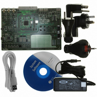
Manufacturer Part Number
EVB9S12XEP100
Description
BOARD EVAL FOR MC9S12XEP100
Manufacturer
Freescale Semiconductor
Type
MCUr
Datasheet
1.EVB9S12XEP100.pdf
(1328 pages)
Specifications of EVB9S12XEP100
Contents
Module and Misc Hardware
Processor To Be Evaluated
MC9S12XEP100
Data Bus Width
16 bit
Interface Type
RS-232
Silicon Manufacturer
Freescale
Core Architecture
S12
Core Sub-architecture
S12
Silicon Core Number
MC9S12
Silicon Family Name
S12XE
Rohs Compliant
Yes
For Use With/related Products
MC9S12XEP100
Lead Free Status / RoHS Status
Lead free / RoHS Compliant


Freescale Semiconductor
PLLSEL
Because of an order from the United States International Trade Commission, BGA-packaged product lines and partnumbers
CLKSW
UNSEC
indicated here currently are not available from Freescale for import or sale in the United States prior to September 2010
Field
0
0
1
1
2
1
CLKSW
Clock Switch — The CLKSW bit controls which clock the BDM operates with. It is only writable from a hardware
BDM command. A minimum delay of 150 cycles at the clock speed that is active during the data portion of the
command send to change the clock source should occur before the next command can be send. The delay
should be obtained no matter which bit is modified to effectively change the clock source (either PLLSEL bit or
CLKSW bit). This guarantees that the start of the next BDM command uses the new clock for timing subsequent
BDM communications.
Table 7-4
module, the bit is part of the CLKSEL register) bits.
Note: The BDM alternate clock source can only be selected when CLKSW = 0 and PLLSEL = 1. The BDM serial
Note: If the acknowledge function is turned on, changing the CLKSW bit will cause the ACK to be at the new
Note: In emulation modes (if modes available), the CLKSW bit will be set out of RESET.
Unsecure — If the device is secured this bit is only writable in special single chip mode from the BDM secure
firmware. It is in a zero state as secure mode is entered so that the secure BDM firmware lookup table is enabled
and put into the memory map overlapping the standard BDM firmware lookup table.
The secure BDM firmware lookup table verifies that the non-volatile memories (e.g. on-chip EEPROM and/or
Flash EEPROM) are erased. This being the case, the UNSEC bit is set and the BDM program jumps to the start
of the standard BDM firmware lookup table and the secure BDM firmware lookup table is turned off. If the erase
test fails, the UNSEC bit will not be asserted.
0 System is in a secured mode.
1 System is in a unsecured mode.
Note: When UNSEC is set, security is off and the user can change the state of the secure bits in the on-chip
0
1
0
1
interface is now fully synchronized to the alternate clock source, when enabled. This eliminates frequency
restriction on the alternate clock which was required on previous versions. Refer to the device
specification to determine which clock connects to the alternate clock source input.
rate for the write command which changes it.
Flash EEPROM. Note that if the user does not change the state of the bits to “unsecured” mode, the
system will be secured again when it is next taken out of reset.After reset this bit has no meaning or effect
when the security byte in the Flash EEPROM is configured for unsecure mode.
Bus clock dependent on oscillator
Bus clock dependent on oscillator
Alternate clock (refer to the device specification to determine the alternate clock source)
Bus clock dependent on the PLL
shows the resulting BDM clock source based on the CLKSW and the PLLSEL (PLL select in the CRG
Table 7-3. BDMSTS Field Descriptions (continued)
MC9S12XE-Family Reference Manual Rev. 1.23
Table 7-4. BDM Clock Sources
Description
BDMCLK
Chapter 7 Background Debug Module (S12XBDMV2)
287
Related parts for EVB9S12XEP100
Image
Part Number
Description
Manufacturer
Datasheet
Request
R

Part Number:
Description:
Manufacturer:
Freescale Semiconductor, Inc
Datasheet:
Part Number:
Description:
Manufacturer:
Freescale Semiconductor, Inc
Datasheet:
Part Number:
Description:
Manufacturer:
Freescale Semiconductor, Inc
Datasheet:
Part Number:
Description:
Manufacturer:
Freescale Semiconductor, Inc
Datasheet:
Part Number:
Description:
Manufacturer:
Freescale Semiconductor, Inc
Datasheet:
Part Number:
Description:
Manufacturer:
Freescale Semiconductor, Inc
Datasheet:
Part Number:
Description:
Manufacturer:
Freescale Semiconductor, Inc
Datasheet:
Part Number:
Description:
Manufacturer:
Freescale Semiconductor, Inc
Datasheet:
Part Number:
Description:
Manufacturer:
Freescale Semiconductor, Inc
Datasheet:
Part Number:
Description:
Manufacturer:
Freescale Semiconductor, Inc
Datasheet:
Part Number:
Description:
Manufacturer:
Freescale Semiconductor, Inc
Datasheet:
Part Number:
Description:
Manufacturer:
Freescale Semiconductor, Inc
Datasheet:
Part Number:
Description:
Manufacturer:
Freescale Semiconductor, Inc
Datasheet:
Part Number:
Description:
Manufacturer:
Freescale Semiconductor, Inc
Datasheet:
Part Number:
Description:
Manufacturer:
Freescale Semiconductor, Inc
Datasheet: