EVB9S12XEP100 Freescale Semiconductor, EVB9S12XEP100 Datasheet - Page 802
EVB9S12XEP100
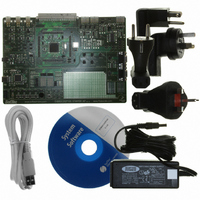
Manufacturer Part Number
EVB9S12XEP100
Description
BOARD EVAL FOR MC9S12XEP100
Manufacturer
Freescale Semiconductor
Type
MCUr
Datasheet
1.EVB9S12XEP100.pdf
(1328 pages)
Specifications of EVB9S12XEP100
Contents
Module and Misc Hardware
Processor To Be Evaluated
MC9S12XEP100
Data Bus Width
16 bit
Interface Type
RS-232
Silicon Manufacturer
Freescale
Core Architecture
S12
Core Sub-architecture
S12
Silicon Core Number
MC9S12
Silicon Family Name
S12XE
Rohs Compliant
Yes
For Use With/related Products
MC9S12XEP100
Lead Free Status / RoHS Status
Lead free / RoHS Compliant


Chapter 22 Timer Module (TIM16B8CV2) Block Description
To operate the 16-bit pulse accumulator independently of input capture or output compare 7 and 0
respectively the user must set the corresponding bits IOSx = 1, OMx = 0 and OLx = 0. OC7M7 in the
OC7M register must also be cleared.
To enable output action using the OM7 and OL7 bits on the timer port,the corresponding bit OC7M7 in
the OC7M register must also be cleared. The settings for these bits can be seen in
Note: in
IOSx is the register TIOS bit x,
OC7Mx is the register OC7M bit x,
TCx is timer Input Capture/Output Compare register,
IOCx is channel x,
OMx/OLx is the register TCTL1/TCTL2,
OC7Dx is the register OC7D bit x.
IOCx = OC7Dx+ OMx/OLx, means that both OC7 event and OCx event will change channel x value.
22.3.2.9
802
Module Base + 0x000A
Module Base + 0x000B
IOCx=OC7Dx
IOC7=OM7/O
Because of an order from the United States International Trade Commission, BGA-packaged product lines and partnumbers
TC7=TCx
Reset
Reset
indicated here currently are not available from Freescale for import or sale in the United States prior to September 2010
L7
W
W
R
R
Table
OC7Mx=1
EDG7B
EDG3B
Timer Control Register 3/Timer Control Register 4 (TCTL3 and TCTL4)
0
0
7
7
IOCx=OC7Dx
IOC7=OM7/O
22-10, the IOS7 and IOSx should be set to 1
+OMx/OLx
TC7>TCx
L7
OC7M7=0
EDG7A
EDG3A
0
0
6
6
TC7=TCx
Figure 22-16. Timer Control Register 3 (TCTL3)
Figure 22-17. Timer Control Register 4 (TCTL4)
Table 22-10. The OC7 and OCx event priority
MC9S12XE-Family Reference Manual Rev. 1.23
IOC7=OM7/OL7
IOCx=OMx/OLx
OC7Mx=0
EDG6B
EDG2B
5
0
5
0
TC7>TCx
EDG6A
EDG2A
0
0
4
4
IOC7=OC7D7
IOCx=OC7Dx
TC7=TCx
EDG5B
EDG1B
OC7Mx=1
0
0
3
3
IOCx=OC7Dx
IOC7=OC7D7
+OMx/OLx
TC7>TCx
EDG5A
EDG1A
OC7M7=1
2
0
2
0
TC7=TCx
Table 22-10
EDG4B
EDG0B
Freescale Semiconductor
IOCx=OMx/OLx
IOC7=OC7D7
0
0
1
1
OC7Mx=0
TC7>TCx
EDG4A
EDG0A
0
0
0
0
Related parts for EVB9S12XEP100
Image
Part Number
Description
Manufacturer
Datasheet
Request
R

Part Number:
Description:
Manufacturer:
Freescale Semiconductor, Inc
Datasheet:
Part Number:
Description:
Manufacturer:
Freescale Semiconductor, Inc
Datasheet:
Part Number:
Description:
Manufacturer:
Freescale Semiconductor, Inc
Datasheet:
Part Number:
Description:
Manufacturer:
Freescale Semiconductor, Inc
Datasheet:
Part Number:
Description:
Manufacturer:
Freescale Semiconductor, Inc
Datasheet:
Part Number:
Description:
Manufacturer:
Freescale Semiconductor, Inc
Datasheet:
Part Number:
Description:
Manufacturer:
Freescale Semiconductor, Inc
Datasheet:
Part Number:
Description:
Manufacturer:
Freescale Semiconductor, Inc
Datasheet:
Part Number:
Description:
Manufacturer:
Freescale Semiconductor, Inc
Datasheet:
Part Number:
Description:
Manufacturer:
Freescale Semiconductor, Inc
Datasheet:
Part Number:
Description:
Manufacturer:
Freescale Semiconductor, Inc
Datasheet:
Part Number:
Description:
Manufacturer:
Freescale Semiconductor, Inc
Datasheet:
Part Number:
Description:
Manufacturer:
Freescale Semiconductor, Inc
Datasheet:
Part Number:
Description:
Manufacturer:
Freescale Semiconductor, Inc
Datasheet:
Part Number:
Description:
Manufacturer:
Freescale Semiconductor, Inc
Datasheet: