EVB9S12XEP100 Freescale Semiconductor, EVB9S12XEP100 Datasheet - Page 281
EVB9S12XEP100
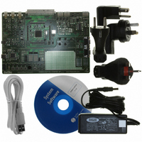
Manufacturer Part Number
EVB9S12XEP100
Description
BOARD EVAL FOR MC9S12XEP100
Manufacturer
Freescale Semiconductor
Type
MCUr
Datasheet
1.EVB9S12XEP100.pdf
(1328 pages)
Specifications of EVB9S12XEP100
Contents
Module and Misc Hardware
Processor To Be Evaluated
MC9S12XEP100
Data Bus Width
16 bit
Interface Type
RS-232
Silicon Manufacturer
Freescale
Core Architecture
S12
Core Sub-architecture
S12
Silicon Core Number
MC9S12
Silicon Family Name
S12XE
Rohs Compliant
Yes
For Use With/related Products
MC9S12XEP100
Lead Free Status / RoHS Status
Lead free / RoHS Compliant


Chapter 7
Background Debug Module (S12XBDMV2)
7.1
This section describes the functionality of the background debug module (BDM) sub-block of the
HCS12X core platform.
The background debug module (BDM) sub-block is a single-wire, background debug system implemented
in on-chip hardware for minimal CPU intervention. All interfacing with the BDM is done via the BKGD
pin.
The BDM has enhanced capability for maintaining synchronization between the target and host while
allowing more flexibility in clock rates. This includes a sync signal to determine the communication rate
and a handshake signal to indicate when an operation is complete. The system is backwards compatible to
the BDM of the S12 family with the following exceptions:
7.1.1
The BDM includes these distinctive features:
Freescale Semiconductor
Revision
Because of an order from the United States International Trade Commission, BGA-packaged product lines and partnumbers
Number
V02.00
V02.01
indicated here currently are not available from Freescale for import or sale in the United States prior to September 2010
•
•
•
•
•
•
•
•
•
•
•
•
TAGGO command no longer supported by BDM
External instruction tagging feature now part of DBG module
BDM register map and register content extended/modified
Global page access functionality
Enabled but not active out of reset in emulation modes (if modes available)
CLKSW bit set out of reset in emulation modes (if modes available).
Family ID readable from firmware ROM at global address 0x7FFF0F (value for HCS12X devices
is 0xC1)
Single-wire communication with host development system
Enhanced capability for allowing more flexibility in clock rates
SYNC command to determine communication rate
GO_UNTIL command
Hardware handshake protocol to increase the performance of the serial communication
Introduction
Revision Date
Features
14 May 2008
07 Mar 2006
Sections
Affected
MC9S12XE-Family Reference Manual , Rev. 1.23
Table 7-1. Revision History
- First version of S12XBDMV2
- Introduced standardized Revision History Table
Description of Changes
281
Related parts for EVB9S12XEP100
Image
Part Number
Description
Manufacturer
Datasheet
Request
R

Part Number:
Description:
Manufacturer:
Freescale Semiconductor, Inc
Datasheet:
Part Number:
Description:
Manufacturer:
Freescale Semiconductor, Inc
Datasheet:
Part Number:
Description:
Manufacturer:
Freescale Semiconductor, Inc
Datasheet:
Part Number:
Description:
Manufacturer:
Freescale Semiconductor, Inc
Datasheet:
Part Number:
Description:
Manufacturer:
Freescale Semiconductor, Inc
Datasheet:
Part Number:
Description:
Manufacturer:
Freescale Semiconductor, Inc
Datasheet:
Part Number:
Description:
Manufacturer:
Freescale Semiconductor, Inc
Datasheet:
Part Number:
Description:
Manufacturer:
Freescale Semiconductor, Inc
Datasheet:
Part Number:
Description:
Manufacturer:
Freescale Semiconductor, Inc
Datasheet:
Part Number:
Description:
Manufacturer:
Freescale Semiconductor, Inc
Datasheet:
Part Number:
Description:
Manufacturer:
Freescale Semiconductor, Inc
Datasheet:
Part Number:
Description:
Manufacturer:
Freescale Semiconductor, Inc
Datasheet:
Part Number:
Description:
Manufacturer:
Freescale Semiconductor, Inc
Datasheet:
Part Number:
Description:
Manufacturer:
Freescale Semiconductor, Inc
Datasheet:
Part Number:
Description:
Manufacturer:
Freescale Semiconductor, Inc
Datasheet: