EVB9S12XEP100 Freescale Semiconductor, EVB9S12XEP100 Datasheet - Page 821
EVB9S12XEP100
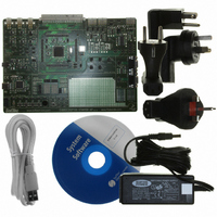
Manufacturer Part Number
EVB9S12XEP100
Description
BOARD EVAL FOR MC9S12XEP100
Manufacturer
Freescale Semiconductor
Type
MCUr
Datasheet
1.EVB9S12XEP100.pdf
(1328 pages)
Specifications of EVB9S12XEP100
Contents
Module and Misc Hardware
Processor To Be Evaluated
MC9S12XEP100
Data Bus Width
16 bit
Interface Type
RS-232
Silicon Manufacturer
Freescale
Core Architecture
S12
Core Sub-architecture
S12
Silicon Core Number
MC9S12
Silicon Family Name
S12XE
Rohs Compliant
Yes
For Use With/related Products
MC9S12XEP100
Lead Free Status / RoHS Status
Lead free / RoHS Compliant


23.2.4
Signals VDDF/VSS are the secondary outputs of VREG_3V3 that provide the power supply for the NVM
logic. These signals are connected to device pins to allow external decoupling capacitors (220 nF, X7R
ceramic).
In Shutdown Mode an external supply driving VDDF/VSS can replace the voltage regulator.
23.2.5
Signals VDDPLL/VSSPLL are the secondary outputs of VREG_3V3 that provide the power supply for
the PLL and oscillator. These signals are connected to device pins to allow external decoupling capacitors
(100 nF...220 nF, X7R ceramic).
In Shutdown Mode, an external supply driving VDDPLL/VSSPLL can replace the voltage regulator.
23.2.6
Signals VDDX/VSS are monitored by VREG_3V3 with the LVR feature.
23.2.7
This optional signal is used to shutdown VREG_3V3. In that case, VDD/VSS and VDDPLL/VSSPLL
must be provided externally. Shutdown mode is entered with VREGEN being low. If VREGEN is high,
the VREG_3V3 is either in Full Performance Mode or in Reduced Power Mode.
For the connectivity of VREGEN, see device specification.
23.2.8
This pin provides the signal selected via APIEA if system is set accordingly. See
Periodical Interrupt Control Register (VREGAPICL)
for details.
For the connectivity of VREG_API, see device specification.
23.3
This section provides a detailed description of all registers accessible in VREG_3V3.
If enabled in the system, the VREG_3V3 will abort all read and write accesses to reserved registers within
it’s memory slice. See device level specification for details.
Freescale Semiconductor
Because of an order from the United States International Trade Commission, BGA-packaged product lines and partnumbers
indicated here currently are not available from Freescale for import or sale in the United States prior to September 2010
Memory Map and Register Definition
VDDF — Regulator Output2 (NVM Logic) Pins
VDDPLL, VSSPLL — Regulator Output3 (PLL) Pins
VDDX — Power Input Pin
VREGEN — Optional Regulator Enable Pin
VREG_API — Optional Autonomous Periodical Interrupt Output Pin
is not supported while MCU is powered.
Switching from FPM or RPM to shutdown of VREG_3V3 and vice versa
MC9S12XE-Family Reference Manual Rev. 1.23
NOTE
and
23.4.8, “Autonomous Periodical Interrupt (API)
Chapter 23 Voltage Regulator (S12VREGL3V3V1)
23.3.2.3, “Autonomous
821
Related parts for EVB9S12XEP100
Image
Part Number
Description
Manufacturer
Datasheet
Request
R

Part Number:
Description:
Manufacturer:
Freescale Semiconductor, Inc
Datasheet:
Part Number:
Description:
Manufacturer:
Freescale Semiconductor, Inc
Datasheet:
Part Number:
Description:
Manufacturer:
Freescale Semiconductor, Inc
Datasheet:
Part Number:
Description:
Manufacturer:
Freescale Semiconductor, Inc
Datasheet:
Part Number:
Description:
Manufacturer:
Freescale Semiconductor, Inc
Datasheet:
Part Number:
Description:
Manufacturer:
Freescale Semiconductor, Inc
Datasheet:
Part Number:
Description:
Manufacturer:
Freescale Semiconductor, Inc
Datasheet:
Part Number:
Description:
Manufacturer:
Freescale Semiconductor, Inc
Datasheet:
Part Number:
Description:
Manufacturer:
Freescale Semiconductor, Inc
Datasheet:
Part Number:
Description:
Manufacturer:
Freescale Semiconductor, Inc
Datasheet:
Part Number:
Description:
Manufacturer:
Freescale Semiconductor, Inc
Datasheet:
Part Number:
Description:
Manufacturer:
Freescale Semiconductor, Inc
Datasheet:
Part Number:
Description:
Manufacturer:
Freescale Semiconductor, Inc
Datasheet:
Part Number:
Description:
Manufacturer:
Freescale Semiconductor, Inc
Datasheet:
Part Number:
Description:
Manufacturer:
Freescale Semiconductor, Inc
Datasheet: