EVB9S12XEP100 Freescale Semiconductor, EVB9S12XEP100 Datasheet - Page 502
EVB9S12XEP100
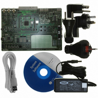
Manufacturer Part Number
EVB9S12XEP100
Description
BOARD EVAL FOR MC9S12XEP100
Manufacturer
Freescale Semiconductor
Type
MCUr
Datasheet
1.EVB9S12XEP100.pdf
(1328 pages)
Specifications of EVB9S12XEP100
Contents
Module and Misc Hardware
Processor To Be Evaluated
MC9S12XEP100
Data Bus Width
16 bit
Interface Type
RS-232
Silicon Manufacturer
Freescale
Core Architecture
S12
Core Sub-architecture
S12
Silicon Core Number
MC9S12
Silicon Family Name
S12XE
Rohs Compliant
Yes
For Use With/related Products
MC9S12XEP100
Lead Free Status / RoHS Status
Lead free / RoHS Compliant


Chapter 12 Pierce Oscillator (S12XOSCLCPV2)
12.1.3
Figure 12-1
12.2
This section lists and describes the signals that connect off chip
12.2.1
Theses pins provides operating voltage (V
allows the supply voltage to the XOSC to use an independent bypass capacitor.
12.2.2
These pins provide the interface for either a crystal or a 1.8V CMOS compatible clock to control the
internal clock generator circuitry. EXTAL is the external clock input or the input to the crystal oscillator
amplifier. XTAL is the output of the crystal oscillator amplifier. The MCU internal system clock is derived
502
Because of an order from the United States International Trade Commission, BGA-packaged product lines and partnumbers
indicated here currently are not available from Freescale for import or sale in the United States prior to September 2010
External Signal Description
Block Diagram
VDDPLL and VSSPLL — Operating and Ground Voltage Pins
EXTAL and XTAL — Input and Output Pins
shows a block diagram of the XOSC.
Detector
Peak
EXTAL
MC9S12XE-Family Reference Manual , Rev. 1.23
Figure 12-1. XOSC Block Diagram
Gain Control
DDPLL
Monitor
Clock
) and ground (V
Rf
V
DDPLL
Monitor_Failure
= 1.8 V
OSCCLK
SSPLL
XTAL
) for the XOSC circuitry. This
Freescale Semiconductor
Related parts for EVB9S12XEP100
Image
Part Number
Description
Manufacturer
Datasheet
Request
R

Part Number:
Description:
Manufacturer:
Freescale Semiconductor, Inc
Datasheet:
Part Number:
Description:
Manufacturer:
Freescale Semiconductor, Inc
Datasheet:
Part Number:
Description:
Manufacturer:
Freescale Semiconductor, Inc
Datasheet:
Part Number:
Description:
Manufacturer:
Freescale Semiconductor, Inc
Datasheet:
Part Number:
Description:
Manufacturer:
Freescale Semiconductor, Inc
Datasheet:
Part Number:
Description:
Manufacturer:
Freescale Semiconductor, Inc
Datasheet:
Part Number:
Description:
Manufacturer:
Freescale Semiconductor, Inc
Datasheet:
Part Number:
Description:
Manufacturer:
Freescale Semiconductor, Inc
Datasheet:
Part Number:
Description:
Manufacturer:
Freescale Semiconductor, Inc
Datasheet:
Part Number:
Description:
Manufacturer:
Freescale Semiconductor, Inc
Datasheet:
Part Number:
Description:
Manufacturer:
Freescale Semiconductor, Inc
Datasheet:
Part Number:
Description:
Manufacturer:
Freescale Semiconductor, Inc
Datasheet:
Part Number:
Description:
Manufacturer:
Freescale Semiconductor, Inc
Datasheet:
Part Number:
Description:
Manufacturer:
Freescale Semiconductor, Inc
Datasheet:
Part Number:
Description:
Manufacturer:
Freescale Semiconductor, Inc
Datasheet: