EVB9S12XEP100 Freescale Semiconductor, EVB9S12XEP100 Datasheet - Page 67
EVB9S12XEP100
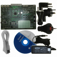
Manufacturer Part Number
EVB9S12XEP100
Description
BOARD EVAL FOR MC9S12XEP100
Manufacturer
Freescale Semiconductor
Type
MCUr
Datasheet
1.EVB9S12XEP100.pdf
(1328 pages)
Specifications of EVB9S12XEP100
Contents
Module and Misc Hardware
Processor To Be Evaluated
MC9S12XEP100
Data Bus Width
16 bit
Interface Type
RS-232
Silicon Manufacturer
Freescale
Core Architecture
S12
Core Sub-architecture
S12
Silicon Core Number
MC9S12
Silicon Family Name
S12XE
Rohs Compliant
Yes
For Use With/related Products
MC9S12XEP100
Lead Free Status / RoHS Status
Lead free / RoHS Compliant


1.2.3.35
PJ5 is a general-purpose input or output pin. It can be configured as a keypad wakeup input. It can be
configured as the serial clock pin SCL of the IIC1 module. It can be also configured as chip-select output 2.
1.2.3.36
PJ4 is a general-purpose input or output pin. It can be configured as a keypad wakeup input. It can be
configured as the serial data pin SDA of the IIC1 module. It can also be configured as chip-select output.
1.2.3.37
PJ3 is a general-purpose input or output pins. It can be configured as a keypad wakeup input.
1.2.3.38
PJ2 is a general-purpose input or output pins. It can be configured as a keypad wakeup input. It can also
be configured as chip-select output.
1.2.3.39
PJ1 is a general-purpose input or output pin. It can be configured as a keypad wakeup input. It can be
configured as the transmit pin TXD of the serial communication interface 2 (SCI2).
1.2.3.40
PJ0 is a general-purpose input or output pin. It can be configured as a keypad wakeup input. It can be
configured as the receive pin RXD of the serial communication interface 2 (SCI2).It can also be configured
as chip-select output 3.
1.2.3.41
PK7 is a general-purpose input or output pin. During MCU emulation modes and normal expanded modes
of operation, this pin is used to enable the Flash EEPROM memory in the memory map (ROMCTL). At
the rising edge of RESET, the state of this pin is latched to the ROMON bit. The EWAIT input signal
maintains the external bus access until the external device is ready to capture data (write) or provide data
(read).
The input voltage threshold for PK7 can be configured to reduced levels, to allow data from an external
3.3-V peripheral to be read by the MCU operating at 5.0 V.
1.2.3.42
PK[6:4] are general-purpose input or output pins. During MCU expanded modes of operation, the
ACC[2:0] signals are used to indicate the access source of the bus cycle. These pins also provide the
expanded addresses ADDR[22:20] for the external bus. In Emulation modes ACC[2:0] is available and is
time multiplexed with the high addresses
Freescale Semiconductor
Because of an order from the United States International Trade Commission, BGA-packaged product lines and partnumbers
indicated here currently are not available from Freescale for import or sale in the United States prior to September 2010
PJ5 / KWJ5 / SCL1 / CS2 — PORT J I/O Pin 5
PJ4 / KWJ4 / SDA1 / CS0 — PORT J I/O Pin 4
PJ3 / KWJ3 — PORT J I/O Pin 3
PJ2 / KWJ2 / CS1 — PORT J I/O Pin 2
PJ1 / KWJ1 / TXD2 — PORT J I/O Pin 1
PJ0 / KWJ0 / RXD2 / CS3 — PORT J I/O Pin 0
PK7 / EWAIT / ROMCTL — Port K I/O Pin 7
PK[6:4] / ADDR[22:20] / ACC[2:0] — Port K I/O Pin [6:4]
MC9S12XE-Family Reference Manual Rev. 1.23
Chapter 1 Device Overview MC9S12XE-Family
67
Related parts for EVB9S12XEP100
Image
Part Number
Description
Manufacturer
Datasheet
Request
R

Part Number:
Description:
Manufacturer:
Freescale Semiconductor, Inc
Datasheet:
Part Number:
Description:
Manufacturer:
Freescale Semiconductor, Inc
Datasheet:
Part Number:
Description:
Manufacturer:
Freescale Semiconductor, Inc
Datasheet:
Part Number:
Description:
Manufacturer:
Freescale Semiconductor, Inc
Datasheet:
Part Number:
Description:
Manufacturer:
Freescale Semiconductor, Inc
Datasheet:
Part Number:
Description:
Manufacturer:
Freescale Semiconductor, Inc
Datasheet:
Part Number:
Description:
Manufacturer:
Freescale Semiconductor, Inc
Datasheet:
Part Number:
Description:
Manufacturer:
Freescale Semiconductor, Inc
Datasheet:
Part Number:
Description:
Manufacturer:
Freescale Semiconductor, Inc
Datasheet:
Part Number:
Description:
Manufacturer:
Freescale Semiconductor, Inc
Datasheet:
Part Number:
Description:
Manufacturer:
Freescale Semiconductor, Inc
Datasheet:
Part Number:
Description:
Manufacturer:
Freescale Semiconductor, Inc
Datasheet:
Part Number:
Description:
Manufacturer:
Freescale Semiconductor, Inc
Datasheet:
Part Number:
Description:
Manufacturer:
Freescale Semiconductor, Inc
Datasheet:
Part Number:
Description:
Manufacturer:
Freescale Semiconductor, Inc
Datasheet: