EVB9S12XEP100 Freescale Semiconductor, EVB9S12XEP100 Datasheet - Page 254
EVB9S12XEP100
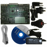
Manufacturer Part Number
EVB9S12XEP100
Description
BOARD EVAL FOR MC9S12XEP100
Manufacturer
Freescale Semiconductor
Type
MCUr
Datasheet
1.EVB9S12XEP100.pdf
(1328 pages)
Specifications of EVB9S12XEP100
Contents
Module and Misc Hardware
Processor To Be Evaluated
MC9S12XEP100
Data Bus Width
16 bit
Interface Type
RS-232
Silicon Manufacturer
Freescale
Core Architecture
S12
Core Sub-architecture
S12
Silicon Core Number
MC9S12
Silicon Family Name
S12XE
Rohs Compliant
Yes
For Use With/related Products
MC9S12XEP100
Lead Free Status / RoHS Status
Lead free / RoHS Compliant


Chapter 5 External Bus Interface (S12XEBIV4)
5.4.2.1
The access source can be determined from the external bus control signals ACC[2:0] as shown in
10.
5.4.2.2
The CPU instruction queue status (execution-start and data-movement information) is brought out as
IQSTAT[3:0] signals. For decoding of the IQSTAT values, refer to the S12X_CPU section.
5.4.2.3
Depending on the access size and alignment, either a word of read data is made visible on the address lines
or only the related data byte will be presented in the ECLK low phase. For details refer to
Invalid IVD are brought out in case of non-CPU read accesses.
5.4.2.4
A bus access lasts 1 ECLK cycle. In case of a stretched external access (emulation expanded mode), up to
an infinite amount of ECLK cycles may be added. ADDRx values will only be shown in ECLK high
phases, while ACCx, IQSTATx, and IVDx values will only be presented in ECLK low phases.
Based on this multiplex timing, ACCx are only shown in the current (first) access cycle. IQSTATx and
(for read accesses) IVDx follow in the next cycle. If the access takes more than one bus cycle, ACCx
display NULL (0x000) in the second and all following cycles of the access. IQSTATx display NULL
(0x0000) from the third until one cycle after the access to indicate continuation.
254
Word read of data at an even and even+1 address
Word read of data at an odd and odd+1 internal RAM address (misaligned)
Byte read of data at an even address
Byte read of data at an odd address
Because of an order from the United States International Trade Commission, BGA-packaged product lines and partnumbers
indicated here currently are not available from Freescale for import or sale in the United States prior to September 2010
Access Source Signals (ACC)
Instruction Queue Status Signals (IQSTAT)
Internal Visibility Data (IVD)
Emulation Modes Timing
1. Denotes also CPU accesses to BDM firmware and BDM registers (IQSTATx
are ‘XXXX’ and RW = 1 in these cases)
Table 5-10. Determining Access Source from Control Signals
ACC[2:0]
110, 111
000
001
010
011
100
101
MC9S12XE-Family Reference Manual , Rev. 1.23
Access
Table 5-11. IVD Read Data Output
Repetition of previous access cycle
CPU access
BDM external access
XGATE PRR access
No access
CPU access error
Reserved
(1)
Access Description
addr[15:8] (rep.)
ivd(odd+1)
IVD[15:8]
ivd(even)
ivd(even)
Freescale Semiconductor
Table
addr[7:0] (rep.)
ivd(even+1)
IVD[7:0]
ivd(odd)
ivd(odd)
Table 5-
5-11.
Related parts for EVB9S12XEP100
Image
Part Number
Description
Manufacturer
Datasheet
Request
R

Part Number:
Description:
Manufacturer:
Freescale Semiconductor, Inc
Datasheet:
Part Number:
Description:
Manufacturer:
Freescale Semiconductor, Inc
Datasheet:
Part Number:
Description:
Manufacturer:
Freescale Semiconductor, Inc
Datasheet:
Part Number:
Description:
Manufacturer:
Freescale Semiconductor, Inc
Datasheet:
Part Number:
Description:
Manufacturer:
Freescale Semiconductor, Inc
Datasheet:
Part Number:
Description:
Manufacturer:
Freescale Semiconductor, Inc
Datasheet:
Part Number:
Description:
Manufacturer:
Freescale Semiconductor, Inc
Datasheet:
Part Number:
Description:
Manufacturer:
Freescale Semiconductor, Inc
Datasheet:
Part Number:
Description:
Manufacturer:
Freescale Semiconductor, Inc
Datasheet:
Part Number:
Description:
Manufacturer:
Freescale Semiconductor, Inc
Datasheet:
Part Number:
Description:
Manufacturer:
Freescale Semiconductor, Inc
Datasheet:
Part Number:
Description:
Manufacturer:
Freescale Semiconductor, Inc
Datasheet:
Part Number:
Description:
Manufacturer:
Freescale Semiconductor, Inc
Datasheet:
Part Number:
Description:
Manufacturer:
Freescale Semiconductor, Inc
Datasheet:
Part Number:
Description:
Manufacturer:
Freescale Semiconductor, Inc
Datasheet: