EVB9S12XEP100 Freescale Semiconductor, EVB9S12XEP100 Datasheet - Page 198
EVB9S12XEP100
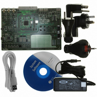
Manufacturer Part Number
EVB9S12XEP100
Description
BOARD EVAL FOR MC9S12XEP100
Manufacturer
Freescale Semiconductor
Type
MCUr
Datasheet
1.EVB9S12XEP100.pdf
(1328 pages)
Specifications of EVB9S12XEP100
Contents
Module and Misc Hardware
Processor To Be Evaluated
MC9S12XEP100
Data Bus Width
16 bit
Interface Type
RS-232
Silicon Manufacturer
Freescale
Core Architecture
S12
Core Sub-architecture
S12
Silicon Core Number
MC9S12
Silicon Family Name
S12XE
Rohs Compliant
Yes
For Use With/related Products
MC9S12XEP100
Lead Free Status / RoHS Status
Lead free / RoHS Compliant


Chapter 3 Memory Mapping Control (S12XMMCV4)
Table 3-7
resources (internal) parameters.
198
Because of an order from the United States International Trade Commission, BGA-packaged product lines and partnumbers
CS3E[1:0]
CS2E[1:0]
CS1E[1:0]
CS0E[1:0]
indicated here currently are not available from Freescale for import or sale in the United States prior to September 2010
Field
7–6
5–4
3–2
1–0
1. External RPAGE accesses in (NX, EX)
2. When ROMHM is set (see ROMHM in
3. When the internal NVM is enabled (see ROMON in
4. External PPAGE accesses in (NX, EX)
chip memory block.
the CS0 is not asserted in the space occupied by this on-chip memory block.
shows the address boundaries of each chip select and the relationship with the implemented
Chip Select 3 Enables — These bits enable the external chip select CS3 output which is asserted during
accesses to specific external addresses. The associated global address range is shown in
Figure
Chip select 3 is only active if enabled in Normal Expanded mode, Emulation Expanded mode.
The function disabled in all other operating modes.
00
01,10,11 Chip select 3 is enabled
Chip Select 2 Enables — These bits enable the external chip select CS2 output which is asserted during
accesses to specific external addresses. The associated global address range is shown in
Figure
Chip select 2 is only active if enabled in Normal Expanded mode, Emulation Expanded mode.
The function disabled in all other operating modes.
00
01,10,11 Chip select 2 is enabled
Chip Select 1 Enables — These bits enable the external chip select CS1 output which is asserted during
accesses to specific external addresses. The associated global address range is shown in
Figure
Chip select 1 is only active if enabled in Normal Expanded mode, Emulation Expanded mode.
The function disabled in all other operating modes.
00
01,10,11 Chip select 1 is enabled
Chip Select 0 Enables — These bits enable the external chip select CS0 output which is asserted during
accesses to specific external addresses. The associated global address range is shown in
Figure
Chip select 0 is only active if enabled in Normal Expanded mode, Emulation Expanded mode.
The function disabled in all other operating modes.
00
01,10,11 Chip select 0 is enabled
Chip Selects
CS2
CS0
CS3
CS1
3-17.
3-17.
3-17.
3-17.
Chip select 3 is disabled
Chip select 2 is disabled
Chip select 1 is disabled
Chip select 0 is disabled
(2)
(3)
Table 3-7. Global Chip Selects Memory Space
MC9S12XE-Family Reference Manual , Rev. 1.23
Table 3-6. MMCCTL0 Field Descriptions
Bottom Address
0x00_0800
0x14_0000
0x20_0000
0x40_0000
Table
3-16) the CS2 is asserted in the space occupied by this on-
Section 3.3.2.5, “MMC Control Register
Description
0x7F_FFFF minus FLASHSIZE
0x0F_FFFF minus RAMSIZE
Top Address
0x1F_FFFF
0x3F_FFFF
Freescale Semiconductor
(MMCCTL1))
Table 3-7
Table 3-7
Table 3-7
Table 3-7
(1)
(4)
and
and
and
and
Related parts for EVB9S12XEP100
Image
Part Number
Description
Manufacturer
Datasheet
Request
R

Part Number:
Description:
Manufacturer:
Freescale Semiconductor, Inc
Datasheet:
Part Number:
Description:
Manufacturer:
Freescale Semiconductor, Inc
Datasheet:
Part Number:
Description:
Manufacturer:
Freescale Semiconductor, Inc
Datasheet:
Part Number:
Description:
Manufacturer:
Freescale Semiconductor, Inc
Datasheet:
Part Number:
Description:
Manufacturer:
Freescale Semiconductor, Inc
Datasheet:
Part Number:
Description:
Manufacturer:
Freescale Semiconductor, Inc
Datasheet:
Part Number:
Description:
Manufacturer:
Freescale Semiconductor, Inc
Datasheet:
Part Number:
Description:
Manufacturer:
Freescale Semiconductor, Inc
Datasheet:
Part Number:
Description:
Manufacturer:
Freescale Semiconductor, Inc
Datasheet:
Part Number:
Description:
Manufacturer:
Freescale Semiconductor, Inc
Datasheet:
Part Number:
Description:
Manufacturer:
Freescale Semiconductor, Inc
Datasheet:
Part Number:
Description:
Manufacturer:
Freescale Semiconductor, Inc
Datasheet:
Part Number:
Description:
Manufacturer:
Freescale Semiconductor, Inc
Datasheet:
Part Number:
Description:
Manufacturer:
Freescale Semiconductor, Inc
Datasheet:
Part Number:
Description:
Manufacturer:
Freescale Semiconductor, Inc
Datasheet: