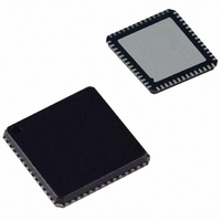
ADUC847BCPZ8-5 Analog Devices Inc, ADUC847BCPZ8-5 Datasheet - Page 100

ADUC847BCPZ8-5
Manufacturer Part Number
ADUC847BCPZ8-5
Description
IC,Data Acquisition CODEC,2-CHANNEL,LLCC,56PIN,PLASTIC
Manufacturer
Analog Devices Inc
Series
MicroConverter® ADuC8xxr
Datasheet
1.EVAL-ADUC845QSZ.pdf
(108 pages)
Specifications of ADUC847BCPZ8-5
Core Processor
8052
Core Size
8-Bit
Speed
12.58MHz
Connectivity
I²C, SPI, UART/USART
Peripherals
POR, PSM, PWM, Temp Sensor, WDT
Number Of I /o
34
Program Memory Size
8KB (8K x 8)
Program Memory Type
FLASH
Eeprom Size
4K x 8
Ram Size
2.25K x 8
Voltage - Supply (vcc/vdd)
4.75 V ~ 5.25 V
Data Converters
A/D 10x24b; D/A 1x12b, 2x16b
Oscillator Type
Internal
Operating Temperature
-40°C ~ 85°C
Package / Case
56-LFCSP
Lead Free Status / RoHS Status
Lead free / RoHS Compliant
For Use With
EVAL-ADUC847QSZ - KIT DEV QUICK START FOR ADUC847
Lead Free Status / RoHS Status
Lead free / RoHS Compliant
- Current page: 100 of 108
- Download datasheet (2Mb)
ADuC845/ADuC847/ADuC848
Table 69. SPI MASTER MODE TIMING (CPHA = 0) Parameter
t
t
t
t
t
t
t
t
t
t
1
SL
SH
DAV
DOSU
DSU
DHD
DF
DR
SR
SF
Characterized under the following conditions:
a. Core clock divider bits CD2, CD1, and CD0 in PLLCON SFR set to 0, 1, and 1, respectively, that is, core clock frequency = 1.57 MHz.
b. SPI bit-rate selection bits SPR1 and SPR0 in SPICON SFR set to 0 and 0, respectively.
(CPOL = 0)
(CPOL = 1)
SCLOCK Low Pulse Width
SCLOCK High Pulse Width
Data Output Valid After SCLOCK Edge
Data Output Setup Before SCLOCK Edge
Data Input Setup Time Before SCLOCK Edge
Data Input Hold Time After SCLOCK Edge
Data Output Fall Time
Data Output Rise Time
SCLOCK Rise Time
SCLOCK Fall Time
SCLOCK
SCLOCK
MOSI
MISO
t
DOSU
t
DSU
MSB IN
1
1
MSB
t
DHD
t
SH
t
DF
Figure 77. SPI Master Mode Timing (CHPA = 0)
t
DAV
t
SL
Rev. B | Page 100 of 108
t
DR
BITS 6–1
BITS 6–1
LSB IN
t
SR
LSB
Min
100
100
t
SF
Typ
635
635
10
10
10
10
Max
50
150
25
25
25
25
Unit
ns
ns
ns
ns
ns
ns
ns
ns
ns
ns
Related parts for ADUC847BCPZ8-5
Image
Part Number
Description
Manufacturer
Datasheet
Request
R

Part Number:
Description:
±1.7g Dual-Axis IMEMS Accelerometer Evaluation Board
Manufacturer:
Analog Devices Inc
Datasheet:

Part Number:
Description:
Inertial Sensor Evaluation System
Manufacturer:
Analog Devices Inc
Datasheet:

Part Number:
Description:
Manufacturer:
Analog Devices Inc
Datasheet:

Part Number:
Description:
Manufacturer:
Analog Devices Inc
Datasheet:

Part Number:
Description:
Manufacturer:
Analog Devices Inc
Datasheet:

Part Number:
Description:
Manufacturer:
Analog Devices Inc
Datasheet:

Part Number:
Description:
Manufacturer:
Analog Devices Inc
Datasheet:

Part Number:
Description:
Manufacturer:
Analog Devices Inc
Datasheet:

Part Number:
Description:
Manufacturer:
Analog Devices Inc
Datasheet:

Part Number:
Description:
Manufacturer:
Analog Devices Inc
Datasheet:

Part Number:
Description:
Manufacturer:
Analog Devices Inc
Datasheet:

Part Number:
Description:
Manufacturer:
Analog Devices Inc
Datasheet:

Part Number:
Description:
Manufacturer:
Analog Devices Inc
Datasheet:


