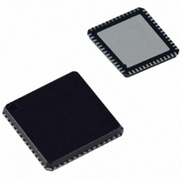
ADUC847BCPZ8-5 Analog Devices Inc, ADUC847BCPZ8-5 Datasheet - Page 73

ADUC847BCPZ8-5
Manufacturer Part Number
ADUC847BCPZ8-5
Description
IC,Data Acquisition CODEC,2-CHANNEL,LLCC,56PIN,PLASTIC
Manufacturer
Analog Devices Inc
Series
MicroConverter® ADuC8xxr
Datasheet
1.EVAL-ADUC845QSZ.pdf
(108 pages)
Specifications of ADUC847BCPZ8-5
Core Processor
8052
Core Size
8-Bit
Speed
12.58MHz
Connectivity
I²C, SPI, UART/USART
Peripherals
POR, PSM, PWM, Temp Sensor, WDT
Number Of I /o
34
Program Memory Size
8KB (8K x 8)
Program Memory Type
FLASH
Eeprom Size
4K x 8
Ram Size
2.25K x 8
Voltage - Supply (vcc/vdd)
4.75 V ~ 5.25 V
Data Converters
A/D 10x24b; D/A 1x12b, 2x16b
Oscillator Type
Internal
Operating Temperature
-40°C ~ 85°C
Package / Case
56-LFCSP
Lead Free Status / RoHS Status
Lead free / RoHS Compliant
For Use With
EVAL-ADUC847QSZ - KIT DEV QUICK START FOR ADUC847
Lead Free Status / RoHS Status
Lead free / RoHS Compliant
8052-COMPATIBLE ON-CHIP PERIPHERALS
This section gives a brief overview of the various secondary
peripheral circuits that are available to the user on-chip. These
features are mostly 8052-compatible (with a few additional
features) and are controlled via standard 8052 SFR bit definitions.
Parallel I/O
The ADuC845/ADuC847/ADuC848 use four input/output
ports to exchange data with external devices. In addition to
performing general-purpose I/O, some are capable of external
memory operations, while others are multiplexed with alternate
functions for the peripheral functions available on-chip. In
general, when a peripheral is enabled, that pin cannot be used
as a general-purpose I/O pin.
Port 0
Port 0 is an 8-bit open-drain bidirectional I/O port that is
directly controlled via the Port 0 SFR (80H). Port 0 is also the
multiplexed low-order address and data bus during accesses to
external data memory.
Figure 48 shows a typical bit latch and I/O buffer for a Port 0
pin. The bit latch (one bit in the port’s SFR) is represented as a
Type D flip-flop, which clocks in a value from the internal bus
in response to a write to latch signal from the CPU. The
Q output of the flip-flop is placed on the internal bus in
response to a read latch signal from the CPU. The level of the
port pin itself is placed on the internal bus in response to a read
pin signal from the CPU. Some instructions that read a port
activate the read latch signal, and others activate the read pin
signal. See the Read-Modify-Write Instructions section for
details.
As shown in Figure 48, the output drivers of Port 0 pins are
switchable to an internal ADDR and ADDR/DATA bus by an
internal control signal for use in external memory accesses.
During external memory accesses, the P0 SFR has 1s written to
it; therefore, all its bit latches become 1. When accessing
external memory, the control signal in Figure 48 goes high,
enabling push-pull operation of the output pin from the internal
address or data bus (ADDR/DATA line). Therefore, no external
pull-ups are required on Port 0 for it to access external memory.
INTERNAL
TO LATCH
LATCH
WRITE
READ
READ
BUS
PIN
Figure 48. Port 0 Bit Latch and I/O Buffer
LATCH
D
CL
Q
Q
ADDR/DATA
CONTROL
DV DD
P0.x
PIN
Rev. B | Page 73 of 108
In general-purpose I/O port mode, Port 0 pins that have 1s
written to them via the Port 0 SFR are configured as open-drain
and, therefore, float. In this state, Port 0 pins can be used as
high impedance inputs. This is represented in Figure 48 by the
NAND gate whose output remains high as long as the control
signal is low, thereby disabling the top FET. External pull-up
resistors are, therefore, required when Port 0 pins are used as
general-purpose outputs. Port 0 pins with 0s written to them
drive a logic low output voltage (V
1.6 mA.
Port 1
Port 1 is also an 8-bit port directly controlled via the P1 SFR
(90H). Port 1 digital output capability is not supported on this
device. Port 1 pins can be configured as digital inputs or analog
inputs. By (power-on) default, these pins are configured as
analog inputs, that is, 1 is written to the corresponding Port 1
register bit. To configure any of these pins as digital inputs, the
user should write a 0 to these port bits to configure the corre-
sponding pin as a high impedance digital input. These pins also
have various secondary functions aside from their analog input
capability, as described in Table 46.
Table 46. Port 1 Alternate Functions
Pin No.
P1.2
P1.3
P1.6
P1.7
Port 2
Port 2 is a bidirectional port with internal pull-up resistors
directly controlled via the P2 SFR. Port 2 also emits the middle-
and high-order address bytes during accesses to the 24-bit
external data memory space.
In general-purpose I/O port mode, Port 2 pins that have 1s
written to them are pulled high by the internal pull-ups as
shown in Figure 50 and, in that state, can be used as inputs. As
inputs, Port 2 pins pulled externally low source current because
of the internal pull-up resistors. Port 2 pins with 0s written to
them drive a logic low output voltage (V
sinking 1.6 mA.
INTERNAL
TO LATCH
Alternate Function
REFIN2+ (second reference input, +’ve)
REFIN2− (second reference input, –‘ve)
IEXC1 (200 µA excitation current source)
IEXC2 (200 µA excitation current source)
LATCH
WRITE
READ
READ
BUS
PIN
Figure 49. Port 1 Bit Latch and I/O Buffer
ADuC845/ADuC847/ADuC848
TO ADC
LATCH
CL
D
Q
Q
OL
) and are capable of sinking
OL
) and are capable of
P1.x
PIN


