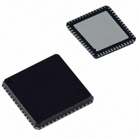
ADUC847BCPZ8-5 Analog Devices Inc, ADUC847BCPZ8-5 Datasheet - Page 11

ADUC847BCPZ8-5
Manufacturer Part Number
ADUC847BCPZ8-5
Description
IC,Data Acquisition CODEC,2-CHANNEL,LLCC,56PIN,PLASTIC
Manufacturer
Analog Devices Inc
Series
MicroConverter® ADuC8xxr
Datasheet
1.EVAL-ADUC845QSZ.pdf
(108 pages)
Specifications of ADUC847BCPZ8-5
Core Processor
8052
Core Size
8-Bit
Speed
12.58MHz
Connectivity
I²C, SPI, UART/USART
Peripherals
POR, PSM, PWM, Temp Sensor, WDT
Number Of I /o
34
Program Memory Size
8KB (8K x 8)
Program Memory Type
FLASH
Eeprom Size
4K x 8
Ram Size
2.25K x 8
Voltage - Supply (vcc/vdd)
4.75 V ~ 5.25 V
Data Converters
A/D 10x24b; D/A 1x12b, 2x16b
Oscillator Type
Internal
Operating Temperature
-40°C ~ 85°C
Package / Case
56-LFCSP
Lead Free Status / RoHS Status
Lead free / RoHS Compliant
For Use With
EVAL-ADUC847QSZ - KIT DEV QUICK START FOR ADUC847
Lead Free Status / RoHS Status
Lead free / RoHS Compliant
PIN CONFIGURATIONS AND FUNCTION DESCRIPTIONS
P1.2/AIN3/REFIN2+
P1.3/AIN4/REFIN2–
Table 3. Pin Fu
P
52-MQFP
1
2
3
4
5
6
---
7
8
Footnotes at end of table.
in No:
P1.6/AIN7/IEXC1
P1.7/AIN8/IEXC2
AINCOM/DAC
P1.0/AIN1
P1.1/AIN2
P1.4/AIN5
P1.5/AIN6
REFIN–
REFIN+
AGND
AV
DD
Pin No: 56-
LFCSP
56
1
2
3
4
5
6
7
8
10
11
12
13
Figure 2. 52-Lead MQFP Pin Configuration
1
2
3
4
5
6
7
8
9
nction Descriptions
14 15 16 17 18 19 20 21 22 23 24 25 26
52 51 50 49 48
ADuC845/ADuC847/ADuC848
PIN 1
IDENTIFIER
(Not to Scale)
Mnemonic
P1.0/AIN1
P1.1/AIN2
P1.2/AIN3/REFIN2+
P1.3/AIN4/REFIN2−
AV
AGND
AGND
REFIN−
REFIN+
TOP VIEW
47 46 45 44
DD
43 42 41 40
39
38
37
36
35
34
33
32
31
30
29
28
27
P2.7/PWMCLK
P2.6/PWM1
P2.5/PWM0
P2.4/T2EX
DGND
P2.3/SS/T2
P2.2/MISO
P2.1/MOSI
P2.0/SCLOCK (SPI)
SDATA
DV
XTAL2
XTAL1
I
I
Type
I
I
S
S
S
I
I
DD
1
Rev. B | Page 11 of 108
Description
B
AIN1 can be u
the positive input of a fully differential pair when used with AIN2.
P1.0 has no digital output driver. It can function as a digital input for which 0
must be written to the port bit. As a digital input, this pin must be driven high
or low externally.
On power-on default, P1.1/AIN2 is configured as the AIN2 analog input.
AIN2 can be used as a pseudo differential input when used with AINCOM or as
the negative input of a fully differential pair when used with AIN1.
P1.1 has no digital output driver. It can function as a digital input for which 0
must be written to the port bit. As a digital input, this pin must be driven high
or low externally.
On power-on default, P1.2/AIN3 is configured as the AIN3 analog input.
AIN3 can be used as a pseudo differential input when used with AINCOM or as
the positive input of a fully differential pair when used with AIN4.
P1.2 has no digital output driver. It can function as a digital input for which 0
must be written to the port bit. As a digital input, this pin must be driven high
or low externally. This pin also functions as a second external differential
reference input, positive terminal.
On power-on default, P1.3/AIN4 is configured as the AIN4 analog input.
AIN4 can be used as a pseudo differential input when used with AINCOM or as
the negative input of a fully differential pair when used with AIN3.
P1.3 has no digital output driver. It can function as a digital input for which 0
must be written to the port bit. As a digital input, this pin must be driven high
or low externally. This pin also functions as a second external differential
reference input, negative terminal.
Analog Supply Voltage.
Analog Ground.
A second analog ground is provided with the LFCSP version only.
External Differential
External Differential Reference Input, Positive Terminal.
y power-on default, P1.0/AIN1 is configured as the AIN1 analog input.
P1.2/AIN3/REFIN2+
P1.3/AIN4/REFIN2–
sed as a pseudo differential input when used with AINCOM or as
P1.6/AIN7/IEXC1
P1.7/AIN8/IEXC2
AINCOM/DAC
P1.1/AIN2
P1.4/AIN5
P1.5/AIN6
Reference Input, Negative Terminal.
REFIN–
REFIN+
AGND
AGND
AV
DAC
DD
Figure 3. 56-Lead LFCSP Pin Configuration
10
11
12
13
14
1
2
3
4
5
6
7
8
9
ADuC845/ADuC847/ADuC848
PIN 1
IDENTIFIER
ADuC845/ADuC847/ADuC848
(Not to Scale)
TOP VIEW
42
41
40
39
38
37
36
35
34
33
32
31
30
29
P2.4/T2EX
DGND
P2.7/PWMCLK
P2.6/PWM1
P2.5/PWM0
DGND
DV
XTAL2
XTAL1
P2.3/SS/T2
P2.2/MISO
P2.1/MOSI
P2.0/SCLOCK (SPI)
SDATA
DD


