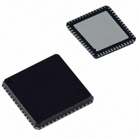
ADUC847BCPZ8-5 Analog Devices Inc, ADUC847BCPZ8-5 Datasheet - Page 49

ADUC847BCPZ8-5
Manufacturer Part Number
ADUC847BCPZ8-5
Description
IC,Data Acquisition CODEC,2-CHANNEL,LLCC,56PIN,PLASTIC
Manufacturer
Analog Devices Inc
Series
MicroConverter® ADuC8xxr
Datasheet
1.EVAL-ADUC845QSZ.pdf
(108 pages)
Specifications of ADUC847BCPZ8-5
Core Processor
8052
Core Size
8-Bit
Speed
12.58MHz
Connectivity
I²C, SPI, UART/USART
Peripherals
POR, PSM, PWM, Temp Sensor, WDT
Number Of I /o
34
Program Memory Size
8KB (8K x 8)
Program Memory Type
FLASH
Eeprom Size
4K x 8
Ram Size
2.25K x 8
Voltage - Supply (vcc/vdd)
4.75 V ~ 5.25 V
Data Converters
A/D 10x24b; D/A 1x12b, 2x16b
Oscillator Type
Internal
Operating Temperature
-40°C ~ 85°C
Package / Case
56-LFCSP
Lead Free Status / RoHS Status
Lead free / RoHS Compliant
For Use With
EVAL-ADUC847QSZ - KIT DEV QUICK START FOR ADUC847
Lead Free Status / RoHS Status
Lead free / RoHS Compliant
F
The ADuC845/ADuC847/ADuC848 contain a 64-kb
Flash/EE pro
memory are a
additional
The upper
contain permanen
serial download, s
emulation. These 2 kbytes of embedded firmware also contain
a pow
brated coef
as ADC, tempera
references.
These 2 kbytes of
code. Attempts t read this space read 0s; therefore, the embed-
ded firmware app
In normal oper ng mode (power-on default), the 62 kbytes of
user Flash/EE p gram memory appear as a single block. This
block is used to st
In normal mode, the 62 kbytes of Flash/EE program memory
can be programmed by serial downloading and by parallel
programming.
LASH/EE PROGRAM MEMORY
KERNEL OR IN PARALLEL PROGRAMMING MODE
PERMANENTLY EMBEDDED DOWNLOAD/DEBUG
PERMANENT
300
250
200
150
100
er-on config
62 kBYTES OF FLASH/EE PROGRAM MEMORY
50
62 kBYTES
CODE TO BE D
ARE AVAILABLE TO THE USER. ALL OF THIS
0
THE KERN
SPACE CAN BE PROGRAMMED FROM THE
Figure 28. Flash/EE Program Memory Map in Normal Mode
EMBEDD
40
NV da
2 kbyte
ficient
INSTRU
gram
vaila
USER PROGRAM MEMORY
Figure 27. Flash/EE Memory Data Retention
50
ED
ati
LY
OF
EL
ro
o
ta memory.
ture sensor, current sources, band gap, and
s to the various calibrated peripherals such
DOWNLOAD/DEBUG KERNEL
EMBEDDED FIRMWARE ALLOWS
CTIONS TO USER CODE.
embedded firmware
ears as NOP instructions to use
ore the user code as shown in Figure 28.
ON-CHIP PROGRAM MEMORY.
erial debug, and nonintrusive single-pin
OWNLOADED TO ANY OF THE
PROGRAM APPEARS AS NOP
s of this Flash/EE program memory array
uration rou
memory. The lower 62 kbytes of this p
ble to the user for program storage or as
tly embedded firmware, allowing in-circuit
T
J
60
JUNCTION TEMPERATURE (°C)
ADI SPECIFICATION
100 YEARS MIN.
AT T
70
tine that downloads factory cali-
J
= 55°C
80
are hidden from the user
90
.
62kBYTE
100
2kBYTE
r code.
FFFFH
F7FFH
F800H
0000H
yte array of
110
rogram
Rev. B | Page 49 of 108
Serial
The ADuC845/ADuC847/ADuC848 facilitate code download
via the standard UART serial port. The parts enter serial down-
load mode after a reset or a power cycle if the PSEN
low through an external 1 kΩ resistor. Once in serial download
mode, the hidden embedded download kernel executes. This
allows the user to download code to the full 62 kbytes of Flash/EE
program memory while the device is in circuit in its target
application hardware.
A PC serial download executable (WSD.EXE) is provided as
part of the ADuC845/ADuC847/ADuC848 Quick Start
development system. Application Note uC004 fully describes
the serial download protocol that is used by the embedded
download kernel. This application note is available at
www.analog.com/microconverter.
Parallel Programming
The
conv
A b
supp
mo
P3
as t
gen
pro
The co
P1.
Tab
P1.4
0
1
0
1
0
1
1
All other codes
de, Ports 0 and 2 operate as the external address bus interface,
operates as the external data bus in
4 are described in Table 31.
he write enable strobe. P1.1, P1.2, P1.3, and P1.4 are used as
lock diagram of the external pin configuration
eral configur
gram and e
le 31. Flash/EE Memory Parallel Programming Modes
parallel programming mo
COMMAND
entional third-par
ort parallel programming is shown in Figure 29. In this
ENABLE
Downloading (In-Circuit Programming)
mmand words that are assigned to P1.1, P1.2, P1.3, and
TIMING
P1.3
0
0
0
0
0
1
1
Port 1 Pins
Figure 29. Flash/EE Memory Parallel Programming
rase operations during parallel programming.
P1.2
0
1
1
1
1
0
0
ation ports that configure the device for various
+5V
ADuC845/ADuC847/ADuC848
ty flash or EEPROM device programmers.
P1.1
0
0
0
1
1
0
1
P1.4–P1.1
P1.7–P1.5
P1.0
ADuC
ADuC847/
ADuC848
Programming Mode
Erase Flash/EE Program, Data, and
Security Mode
Program Code Byte
Program Data Byte
Read Code Byte
Read Data Byte
Program Security Modes
Read/Verify Security Modes
Redundant
de is fully compatible with
845/
P3.7–P3.0
RESET
terface, and P1.0 operates
EA
DATA
required to
pin is pulled
GND
V
DD


