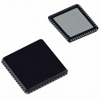
ADUC847BCPZ8-5 Analog Devices Inc, ADUC847BCPZ8-5 Datasheet - Page 58

ADUC847BCPZ8-5
Manufacturer Part Number
ADUC847BCPZ8-5
Description
IC,Data Acquisition CODEC,2-CHANNEL,LLCC,56PIN,PLASTIC
Manufacturer
Analog Devices Inc
Series
MicroConverter® ADuC8xxr
Datasheet
1.EVAL-ADUC845QSZ.pdf
(108 pages)
Specifications of ADUC847BCPZ8-5
Core Processor
8052
Core Size
8-Bit
Speed
12.58MHz
Connectivity
I²C, SPI, UART/USART
Peripherals
POR, PSM, PWM, Temp Sensor, WDT
Number Of I /o
34
Program Memory Size
8KB (8K x 8)
Program Memory Type
FLASH
Eeprom Size
4K x 8
Ram Size
2.25K x 8
Voltage - Supply (vcc/vdd)
4.75 V ~ 5.25 V
Data Converters
A/D 10x24b; D/A 1x12b, 2x16b
Oscillator Type
Internal
Operating Temperature
-40°C ~ 85°C
Package / Case
56-LFCSP
Lead Free Status / RoHS Status
Lead free / RoHS Compliant
For Use With
EVAL-ADUC847QSZ - KIT DEV QUICK START FOR ADUC847
Lead Free Status / RoHS Status
Lead free / RoHS Compliant
ADuC845/ADuC847/ADuC848
Mode 3 (Twin 16-Bit PWM)
In Mode 3, the PWM counter is fixed to count from 0 to 65536,
giving a fixed 16-bit PWM. Operating from the 12.58 MHz core
clock results in a PWM output rate of 192 Hz. The duty cycle of
the PWM outputs at P2.5 and P2.6 are independently
programmable.
As shown in Figure 41, while the PWM counter is less than
PWM0H/L, the output of PWM0 (P2.5) is high. Once the
PWM counter equals PWM0H/L, PWM0 (P2.5) goes low and
remains low until the PWM counter rolls over.
Similarly, while the PWM counter is less than PWM1H/L, the
output of PWM1 (P2.6) is high. Once the PWM counter equals
PWM1H/L, PWM1 (P2.6) goes low and remains low until the
PWM counter rolls over.
In this mode, both PWM outputs are synchronized, that is, once
the PWM counter rolls over to 0, both PWM0 (P2.5) and PWM1
(P2.6) go high.
PWM COUNTER
Figure 41. PWM Mode 3
65536
PWM1H/L
PWM0H/L
0
P2.5
P2.6
Rev. B | Page 58 of 108
Mode 4 (Dual NRZ 16-Bit Σ-∆ DAC)
Mode 4 provides a high speed PWM output similar to that of a
Σ-∆ DAC. Typically, this mode is used with the PWM clock
equal to 12.58 MHz.
In this mode, P1.0 and P1.1 are updated every PWM clock
(80 ns in the case of 12.58 MHz). Over any 65536 cycles (16-bit
PWM), PWM0 (P1.0) is high for PWM0H/L cycles and low for
(65536 – PWM0H/L) cycles. Similarly, PWM1 (P1.1) is high for
PWM1H/L cycles and low for (65536 – PWM1H/L) cycles.
If PWM1H is set to 4010H (slightly above one-quarter of FS),
typically P1.1 is low for three clocks and high for one clock
(each clock is approximately 80 ns). Over every 65536 clocks,
the PWM compromises for the fact that the output should be
slightly above one-quarter of full scale, by having a high cycle
followed by only two low cycles.
For faster DAC outputs (at lower resolution), write 0s to the
LSBs that are not required with a 1 in the LSB position. If, for
example, only 12-bit performance is required, write 0001 to the
4 LSBs. This means that a 12-bit accurate Σ -Δ DAC output can
occur at 3 kHz. Similarly, writing 00000001 to the 8 LSBs gives
an 8-bit accurate Σ-Δ DAC output at 49 kHz.
12.583MHz
PWM0H/L = C000H
PWM1H/L = 4000H
16-BIT
16-BIT
16-BIT
16-BIT
LATCH
Figure 42. PWM Mode 4
CARRY OUT AT P2.5
CARRY OUT AT P2.6
16-BIT
16-BIT
80µs
80µs
0
0
1
1
0
1
1
0
1
0
1
0


