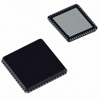
ADUC847BCPZ8-5 Analog Devices Inc, ADUC847BCPZ8-5 Datasheet - Page 23

ADUC847BCPZ8-5
Manufacturer Part Number
ADUC847BCPZ8-5
Description
IC,Data Acquisition CODEC,2-CHANNEL,LLCC,56PIN,PLASTIC
Manufacturer
Analog Devices Inc
Series
MicroConverter® ADuC8xxr
Datasheet
1.EVAL-ADUC845QSZ.pdf
(108 pages)
Specifications of ADUC847BCPZ8-5
Core Processor
8052
Core Size
8-Bit
Speed
12.58MHz
Connectivity
I²C, SPI, UART/USART
Peripherals
POR, PSM, PWM, Temp Sensor, WDT
Number Of I /o
34
Program Memory Size
8KB (8K x 8)
Program Memory Type
FLASH
Eeprom Size
4K x 8
Ram Size
2.25K x 8
Voltage - Supply (vcc/vdd)
4.75 V ~ 5.25 V
Data Converters
A/D 10x24b; D/A 1x12b, 2x16b
Oscillator Type
Internal
Operating Temperature
-40°C ~ 85°C
Package / Case
56-LFCSP
Lead Free Status / RoHS Status
Lead free / RoHS Compliant
For Use With
EVAL-ADUC847QSZ - KIT DEV QUICK START FOR ADUC847
Lead Free Status / RoHS Status
Lead free / RoHS Compliant
Internal XRAM
The ADuC845, ADuC847, and ADuC848 contain 2 kbytes of
on-chip extended data memory. This memory, although on-
chip, is accessed via the MOVX instruction. The 2 kbytes of
internal XRAM are mapped into the bottom 2 kbytes of the
external address space if the CFG84x.0 (Table 7) bit is set;
otherwise, access to the external data memory occurs just like a
standard 8051.
Even with the CFG84x.0 bit set, access to the external (off chip),
XRAM occurs once the 24-bit DPTR is greater than 0007FFH.
When enabled and when accessing the internal XRAM, the P0
and P2 port pin operations, as well as the RD and WR strobes,
do not operate as a standard 8051 MOVX instruction. This
allows the user to use these port pins as standard I/O. The
internal XRAM can be configured as part of the extended 11-bit
stack pointer. By default, the stack operates exactly like an 8052
in that it rolls over from FFH to 00H in the general-purpose
RAM. On the ADuC845, ADuC847, and ADuC848, however, it
BITS IN PSW
SELECTED
BANKS
FFFFFFH
000000H
VIA
Figure 8. Lower 128 Bytes of Internal Data Memory
10
11
01
00
CFG845/7/8.0 = 0
EXTERNAL
AD
Figure 9. Internal and External XRAM
MEMORY
SP
SPACE
(24-BIT
30H
20H
18H
10H
08H
00H
DATA
DRESS
ACE)
7FH
2FH
1FH
17H
0FH
07H
FFFFFFH
0007FFH
000800H
000000H
BIT-ADDRESSABLE
(BIT ADDRESSES)
FOUR BANKS OF EIGHT
REGISTERS
R0 TO R7
GENERAL-PURPOSE
AREA
CFG845/7/8.0 = 1
RESET VALUE OF
STACK POINTER
EXTERNAL
ADDRESS
2 kBYTES
MEMORY
ON-CHIP
SPACE)
SPACE
(24-BIT
DATA
XRAM
Rev. B | Page 23 of 108
is possible (by setting C
enable the 11-bit extended stack pointer. In this case, the stack
rolls over from FFH in RAM to 0100H in XRAM.
The 11-bit stack pointer is visible in the SPH and SP SFRs. Th
SP SFR is located at 81H as with a standard 8052. The SPH SF
is located at B7H. The 3 LSBs of the SPH SFR contain the 3
extra bits nece
SFR into an 11-bit stack pointer.
External Data Memory (External XRAM)
There is no support for external progra
parts. Howeve ju
ADuC845/ADuC847/ADuC
memory using a M
a
access the data memory. The parts, ho
16 Mbytes of external data memory. T
the 64 kb tes of ext
sta
Co
When
to
o
s
EW
SF
Po
Bit A
This s
dictates the number of wait states for the MOVX instruction.
The value can vary between 0H and 7H. The MOVX instruc-
tion increases by one machine cycle (4 + n, where n = EWAIT
number in decimal) for every increase in the EWAIT value.
peeds.
utomatically outputs the various control strobes required to
peration. This is to account
R Address:
be prog mmed to g
wer-On
ndard 8051-compat
nsidera
AIT SFR
ddres
pecial function register (SFR), when programmed,
acce
CFG845/7/8.7 = 0
y
tions
ra
sabl
Defa
ssing exte al RAM, the EWAIT regis
FFH
00H
Figure 10. Extended Stack Pointer Operation
r, st like a standard 8051-compatible core, the
ssary to extend the 8-bit stack pointer in the SP
e:
ult:
section
ON-CHIP DATA
256 BYTES OF
ern
OV
ADuC845/ADuC847/ADuC848
rn
(DATA +
STACK)
al data memor
RAM
ible core. Se
X ins
9FH
00H
No
ive e ra ma
FG845.7/ADuC847.7/ADuC848.7) to
CFG845/7/8.7 = 1
for details.
xt
truction. The MOVX instruction
848 can access external data
for
07FFH
differi
100H
e the Hardware Design
00H
chin
y space available on a
wever, can access up to
his is an enhancement of
ON-CHIP XRAM
ng
(DATA + STACK
m memory access to the
ON-CHIP XRAM
FOR EXSP = 0)
(DATA ONLY)
FOR EXSP = 1,
e cycles to the M
LOWER 256
UPPER 1792
DATA ONLY
BYTES OF
BYTES OF
external RAM access
ter might need
OVX
e
R


