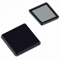
ADUC847BCPZ8-5 Analog Devices Inc, ADUC847BCPZ8-5 Datasheet - Page 18

ADUC847BCPZ8-5
Manufacturer Part Number
ADUC847BCPZ8-5
Description
IC,Data Acquisition CODEC,2-CHANNEL,LLCC,56PIN,PLASTIC
Manufacturer
Analog Devices Inc
Series
MicroConverter® ADuC8xxr
Datasheet
1.EVAL-ADUC845QSZ.pdf
(108 pages)
Specifications of ADUC847BCPZ8-5
Core Processor
8052
Core Size
8-Bit
Speed
12.58MHz
Connectivity
I²C, SPI, UART/USART
Peripherals
POR, PSM, PWM, Temp Sensor, WDT
Number Of I /o
34
Program Memory Size
8KB (8K x 8)
Program Memory Type
FLASH
Eeprom Size
4K x 8
Ram Size
2.25K x 8
Voltage - Supply (vcc/vdd)
4.75 V ~ 5.25 V
Data Converters
A/D 10x24b; D/A 1x12b, 2x16b
Oscillator Type
Internal
Operating Temperature
-40°C ~ 85°C
Package / Case
56-LFCSP
Lead Free Status / RoHS Status
Lead free / RoHS Compliant
For Use With
EVAL-ADUC847QSZ - KIT DEV QUICK START FOR ADUC847
Lead Free Status / RoHS Status
Lead free / RoHS Compliant
ADuC845/ADuC847/ADuC848
8052 INSTRUCTION SET
Table 4 documents the number of clock cycles required for each
instruction. Most instructions are executed in one or two clock
cycles resulting in 12.58 MIPs peak performance when operating
at PLLCON = 00H.
TIMER OPERATION
Timers on a standard 8052 increment by one with each machine
cycle. On the ADuC845, ADuC847, and ADuC848, one
machine cycle is equal to one clock cycle; therefore, the timers
increment at the same rate as the core clock.
AINCOM/DAC
REFIN+
REFIN–
AIN10
IEXC1
IEXC2
AIN1
AIN2
AIN3
AIN4
AIN5
AIN6
AIN7
AIN8
AIN9
56
10
11
12
15
16
13
11
12
1
2
3
9
8
7
NOTES
1. THE PIN NUMBERS REFER TO THE LFCSP PACKAGE ONLY.
200µA
46 47 48 49 52 53 54 55
4
5
CURRENT
SOURCE
MIX
6
MUX
AIN
22
200µA
36 51
REFERENCE
BUF
BAND GAP
23 37 38 50
DETECT
POR
V
REF
PGA
56
Figure 6. Detailed Block Diagram of the ADuC848
1
17
2
11-BIT STACK POINTER
62 kBYTES PROGRAM/
2 × DATA POINTERS
SERIAL PORT
PRIMARY ADC
3
4 kBYTES DATA/
Σ-∆ ADC
18
UART
9
16-BIT
FLASH/EE
FLASH/EE
Rev. B | Page 18 of 108
10
DOWNLOADER
19
DEBUGGER
11 12
ADuC848
CALIBRATION
TIMER
UART
CONTROL
ALE
On the ADuC834, the output on the ALE pin is a clock at 1/6th
of the core operating frequency. On the ADuC845, ADuC847,
and ADuC848, the ALE pin operates as follows. For a single
machine cycle instruction, ALE is high for the entire machine
cycle. For a two or more m
for the first machine cycle and then low for the remainder of the
machine cycles.
EXTERNAL MEMORY ACCESS
The ADuC845, ADuC847, and ADuC848 do not support
external program memory access, but the parts can access up to
16 MB (24 address bits) of external data memory. When
accessing external RAM, the EWAIT register might need to be
programmed in order to give extra machine cycles to MOVX
commands to allow for differing external RAM access speeds.
30 31 32 33 39 40 41 42
ADC
AND
SINGLE-
44 43
CYCLE
CORE
8052
MCU
45
CONTROL
CONTROL
DAC
30
INTERFACE
SPI SERIAL
PWM
POWER SUPPLY
31
WATCHDOG
2304 BYTES
USER RAM
MONITOR
32
TIMER
33
achine cycle instruction, ALE is high
18 19 20 21 24 25 26 27
PLL WITH PROG.
CLOCK DIVIDER
OUTPUT DAC
VOLTAGE
INTERFACE
RTC TIMER
I
WAKE-UP/
2
C SERIAL
12-BIT
Σ-∆ DAC
28
16-BIT
16-BIT
DUAL
DUAL
PWM
29
COUNTER
TIMERS
16-BIT
34
BUF
OSC
MUX
35
14
40
41
42
24
25
33
39
20
21
PWM1
PWMCLK
DAC
PWM0
T0
T1
T2
T2EX
INT0
INT1


