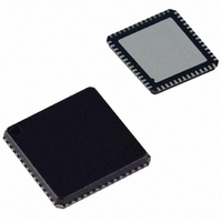
ADUC847BCPZ8-5 Analog Devices Inc, ADUC847BCPZ8-5 Datasheet - Page 12

ADUC847BCPZ8-5
Manufacturer Part Number
ADUC847BCPZ8-5
Description
IC,Data Acquisition CODEC,2-CHANNEL,LLCC,56PIN,PLASTIC
Manufacturer
Analog Devices Inc
Series
MicroConverter® ADuC8xxr
Datasheet
1.EVAL-ADUC845QSZ.pdf
(108 pages)
Specifications of ADUC847BCPZ8-5
Core Processor
8052
Core Size
8-Bit
Speed
12.58MHz
Connectivity
I²C, SPI, UART/USART
Peripherals
POR, PSM, PWM, Temp Sensor, WDT
Number Of I /o
34
Program Memory Size
8KB (8K x 8)
Program Memory Type
FLASH
Eeprom Size
4K x 8
Ram Size
2.25K x 8
Voltage - Supply (vcc/vdd)
4.75 V ~ 5.25 V
Data Converters
A/D 10x24b; D/A 1x12b, 2x16b
Oscillator Type
Internal
Operating Temperature
-40°C ~ 85°C
Package / Case
56-LFCSP
Lead Free Status / RoHS Status
Lead free / RoHS Compliant
For Use With
EVAL-ADUC847QSZ - KIT DEV QUICK START FOR ADUC847
Lead Free Status / RoHS Status
Lead free / RoHS Compliant
ADuC845/ADuC847/ADuC848
Pin No:
52-MQFP
9
10
11
12
13
14
----
----
15
16–
22–25
16
17
18
19
22
23
24
25
19
Pin No: 56-
LFCSP
9
10
11
12
13
14
15
16
17
18–
24–27
18
19
20
21
24
25
26
27
21
Mnemonic
P1.4/AIN5
P1.5/AIN6
P1.6/AIN7/IEXC1
P1.7/AIN8/IEXC2
AINCOM/DAC
DAC
AIN9
AIN10
RESET
P3.0–P3
P3.0/RxD
P3.1/TxD
P3.2/INT0
P3.3/INT1
P3.4/T0
P3.5/T1
P3.6/WR
P3.7/RD
.7
Type
I
I
I/O
I/O
I/O
O
I
I
I
I/O
1
Rev. B | Page 12 of 108
Description
On power-on default, P1.4/AIN5 is configured as the AIN5
AIN5 can be used as a pseudo differential input when us
the positive input of a fully differential pair when used with AIN6.
P1.0 has no digital output driver. It can function as a digital input for whic
must be written to the port bit. As a digital input, this pin must be driven high
or low externally.
On power-on default, P1.5/AIN6 is configured as the AIN6 analog input.
AIN6 can be used as a pseudo differential input when used with AINCOM or as
the negative input
P1.1 has no digital output driver. It can function as a digital input for whic
must be written to the port bit. As a digital input, this pin must be driven high
or low externally.
On power-on default, P1.6/AIN7 is configured as the AIN7 analog input.
AIN7 can be used as a pseudo differential input when used with AINCOM or as
the positive input
current sources can also be configured at this pin.
P1.6 has no digital output driver. It can, however, function as a digital input for
which 0 must be written to the port bit. As a digital input, this pin must be
driven high or low externally.
On power-on default, P1.7/AIN8 is configured as the AIN8 analog input.
AIN8 can be used as a pseudo differential input when used with AINCOM or
the negative input of a fully dif
both current sources can also be configured at this pin.
P1.7 has no digital output driver. It can, however, function as a digital input for
which 0 must be written to the port bit. As a digital input, this pin must be
driven high or low externally.
All analog inputs can be referred to this pin, provided that a relevant pseudo
differential input mode is selected. This pin also functions as an alternative pin
out for the DAC.
The voltage output from the DAC, if enabled, appears at this pin.
AIN9 can be used as a pseudo differential analog input when used with
AINCOM or as the
AIN10 (LFCSP version only).
AIN10 can be used as a pseudo differential analog input when used with
AINCOM or as the negative input of a fully differential pair when used with
AIN9 (LFCSP version only).
Reset Input. A high level on this pin for 16 core clock cycles while the
oscillator is running resets the device. This pin has an internal weak pull-dow
and a Schmitt trigger input stage.
P3.0 to P3.7 are bidirectional port pins with internal pull-up resistors. P
pins that have 1s written to them are pulled high by the internal pull-up
resistors, and in that state can be used as inputs. As inputs, Port 3 pins being
pulled externally low source current because of the internal pull-up resistors
When driving a 0-to-1 output transition, a strong pull-up is active for one cor
clock period of the instruction cycle.
Port 3 pins also have the various secondary functions described below.
Receiver Data for UART Serial Port.
Transmitter Data for UART Serial Port.
External Interrupt 0. This pin can also be used as a gate control input to Time
External Interrupt 1. This pin can also be used as a gate control input to Timer 1.
Timer/Counter 0 External Input.
Timer/Counter 1 External Input.
External Data Memory Write Strobe. This pin latches the data byte from Port 0
into an external data memory.
External Data Memory Read Strobe. This pin enables the data from an external
data memory to Port 0.
of a fully differential pair when used with AIN8. One or both
positive input of a fully differential pair when used with
of a fully differential pair when used with AIN5.
ferential pair when used with AIN7. One or
ed with AINCOM or as
analog input.
ort 3
h 0
h 0
r 0.
as
.
e
n


