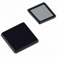
ADUC847BCPZ8-5 Analog Devices Inc, ADUC847BCPZ8-5 Datasheet - Page 88

ADUC847BCPZ8-5
Manufacturer Part Number
ADUC847BCPZ8-5
Description
IC,Data Acquisition CODEC,2-CHANNEL,LLCC,56PIN,PLASTIC
Manufacturer
Analog Devices Inc
Series
MicroConverter® ADuC8xxr
Datasheet
1.EVAL-ADUC845QSZ.pdf
(108 pages)
Specifications of ADUC847BCPZ8-5
Core Processor
8052
Core Size
8-Bit
Speed
12.58MHz
Connectivity
I²C, SPI, UART/USART
Peripherals
POR, PSM, PWM, Temp Sensor, WDT
Number Of I /o
34
Program Memory Size
8KB (8K x 8)
Program Memory Type
FLASH
Eeprom Size
4K x 8
Ram Size
2.25K x 8
Voltage - Supply (vcc/vdd)
4.75 V ~ 5.25 V
Data Converters
A/D 10x24b; D/A 1x12b, 2x16b
Oscillator Type
Internal
Operating Temperature
-40°C ~ 85°C
Package / Case
56-LFCSP
Lead Free Status / RoHS Status
Lead free / RoHS Compliant
For Use With
EVAL-ADUC847QSZ - KIT DEV QUICK START FOR ADUC847
Lead Free Status / RoHS Status
Lead free / RoHS Compliant
ADuC845/ADuC847/ADuC848
as op amps and voltage reference) can be powered from the
AV
Notice that in both Figure 64 and Figure 65 a large value (10 µF)
reservoir capacitor sits on DV
sits on AV
located at each V
practice, be sure to include all of these capacitors and ensure
that the smaller capacitors are closer than the 10 µF capacitors
to each V
the ground terminal of each of these capacitors directly to the
underlying ground plane. Finally, note that, at all times, the
analog and digital ground pins on the part must be referenced
to the same system ground reference point. It is recommended
that the LFCSP paddle be soldered to ensure mechanical
stability but be floated with respect to system V
POWER-ON RESET OPERATION
An internal power-on reset (POR) is implemented on the
ADuC845/ADuC847/ADuC848.
3 V Part
For DV
As DV
typically 128 ms before the part is released from reset. The user
must ensure that the power supply has at least reached a stable
2.7 V minimum level by this time. Likewise on power-down,
the internal POR holds the part in reset until the power supply
drops below 1 V. Figure 66 illustrates the operation of the
internal POR.
DV
CORE RESET
INTERNAL
DD
DD
supply line as well.
2.63V TYP
DD
1.0V TYP
DD
DIGITAL SUPPLY
DD
rises above 2.63 V, an internal timer times out for
DD
below 2.63 V, the internal POR holds the part in reset.
+
–
0.1µF
pin with lead lengths as short as possible. Connect
. Also, local decoupling capacitors (0.1 µF) are
Figure 65. External Single-Supply Connections
DD
Figure 66. 3 V Part POR operation
(56-Lead LFCSP Pin Numbering)
pin of the chip. As per standard design
128ms TYP
10µF
22
36
51
23
37
38
50
DV
DGND
DD
BEAD
DD
ADuC845/
ADuC847/
ADuC848
and a separate 10 µF capacitor
128ms TYP
1.6Ω
AGND
AV
DD
4
5
6
10µF
DD
s or grounds.
0.1µF
1.0V TYP
Rev. B | Page 88 of 108
5 V Part
For DV
As DV
approximately 128 ms before the part is released from reset. The
user must ensure that the power supply has reached a stable
4.75 V minimum level by this time. Likewise on power-down,
the internal POR holds the part in reset until the power supply
drops below 1 V. Figure 67 illustrates this operation.
POWER CONSUMPTION
The DV
normal and power-down modes. The AV
current is specified with the analog peripherals disabled. The
normal mode power consumption represents the current drawn
from DV
(such as the watchdog timer and power supply monitor)
consume negligible current and are therefore included with the
normal operating current. The user must add any currents
sourced by the parallel and serial I/O pins, and those sourced by
the DAC to determine the total current needed at the ADuC845/
ADuC847/ADuC848 DV
drawn from the DV
during Flash/EE erase and program cycles.
POWER-SAVING MODES
Setting the power-down mode bit, PCON.1, in the PCON SFR
described in Table 6, allows the chip to be switched from
normal mode into full power-down mode.
In power-down mode, both the PLL and the clock to the core
are stopped. The on-chip oscillator can be halted or can
continue to oscillate, depending on the state of the oscillator
power-down bit (OSC_PD) in the PLLCON SFR. The TIC,
driven directly from the oscillator, can also be enabled during
power-down. However, all other on-chip peripherals are shut
down. Port pins retain their logic levels in this mode, but the
DAC output goes to a high impedance state (three-state) while
ALE and PSEN outputs are held low. There are five ways to
terminate power-down mode:
•
DV
CORE RESET
INTERNAL
DD
Asserting the RESET Pin
Returns to normal mode. All registers are set to their reset
default value and program execution starts at the reset
vector once the RESET pin is de-asserted.
DD
1.0V TYP
4.5V TYP
DD
DD
DD
rises above 4.5 V, an internal timer times out for
below 4.5 V, the internal POR holds the part in reset.
power supply current consumption is specified in
by the digital core. The other on-chip peripherals
Figure 67. 5 V Part POR Operation
DD
128ms TYP
supply increases by approximately 5 mA
DD
and AV
DD
128ms TYP
supply pins. Also, current
DD
power supply
1.0V TYP


