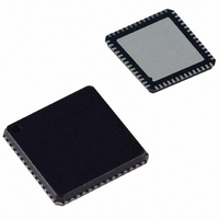
ADUC847BCPZ8-5 Analog Devices Inc, ADUC847BCPZ8-5 Datasheet - Page 42

ADUC847BCPZ8-5
Manufacturer Part Number
ADUC847BCPZ8-5
Description
IC,Data Acquisition CODEC,2-CHANNEL,LLCC,56PIN,PLASTIC
Manufacturer
Analog Devices Inc
Series
MicroConverter® ADuC8xxr
Datasheet
1.EVAL-ADUC845QSZ.pdf
(108 pages)
Specifications of ADUC847BCPZ8-5
Core Processor
8052
Core Size
8-Bit
Speed
12.58MHz
Connectivity
I²C, SPI, UART/USART
Peripherals
POR, PSM, PWM, Temp Sensor, WDT
Number Of I /o
34
Program Memory Size
8KB (8K x 8)
Program Memory Type
FLASH
Eeprom Size
4K x 8
Ram Size
2.25K x 8
Voltage - Supply (vcc/vdd)
4.75 V ~ 5.25 V
Data Converters
A/D 10x24b; D/A 1x12b, 2x16b
Oscillator Type
Internal
Operating Temperature
-40°C ~ 85°C
Package / Case
56-LFCSP
Lead Free Status / RoHS Status
Lead free / RoHS Compliant
For Use With
EVAL-ADUC847QSZ - KIT DEV QUICK START FOR ADUC847
Lead Free Status / RoHS Status
Lead free / RoHS Compliant
ADuC845/ADuC847/ADuC848
Notes on the ADCMODE Register
•
•
•
Any change to the MD bits immediately resets both ADCs
(auxiliary
to the MD2–MD bits w
treated as a re
note of this section.)
If ADC0CON is written when ADC0EN =
ADC0EN is changed from 0 to 1, both AD
imm diately reset. In
given
requested on the primary ADC
to. Only applicable to the AD
On the other hand, if ADC1C
ADC1EN is changed from 0 t
is reset. For example, if the pr
converting when the auxiliary ADC cha e or en
occur
than a
difference from the primar
into step with the outputs of t
is that the first conversion tim or th
delayed by up to three output
update rate is synchronized to
applicable to ADuC845. If the DC1CON wr
after the primary ADC has co
auxiliary ADC can respond im edia y with t havi
fall into step with the primary ADCs
e
s, the p
priority over th
llow
ADC o
the auxiliary ADC
rimary ADC con
set.
0
nly applicab
(See t
e auxilia
other w
he exception to this in the third
ith no change in contents is also
y A
uC845.
ords, the primary ADC is
s w
le to the ADuC845). A write
ry ADC and any change
o 1
im
he pri ary A C. Th esult
ON is writte
tinues undisturbed. Rather
mp
to operate with a phase
e f
DC, the auxiliary ADC falls
A
th
m
is immediately responded
ary AD is cont
hile
, only
e pr
lete ts ope
m
im
d i
the a
tel
e a
ou
the
ary A
C
ng
tput c le.
uxili
uxi
n to or
auxilia
Cs are also
1, or if
D
ary
liar
DC
rat
ite o
ou
yc
ion, t
ADC
y AD
inuously
. Onl
ry ADC
able
if
ccu
e r
he
rs
y
C
ng
is
Rev. B | Page 42 of 108
to
•
•
•
•
•
If the
register, the current ADCMODE bits are preserved, that is,
they are not reset to default state. Upon a subsequent
resumption of normal operating mode, the ADCs restarts
the selected operation defined by the ADCMODE register.
Once ADCMODE has been written with a calibration
mode, the RDY0/1 (ADuC845 only) bits (ADCSTAT) are
reset and the calibration commences. On completion, the
appropriate calibration registers are written, the rele
bits in ADCSTAT are written, and the MD2 MD0 bits a
reset to 000B to indicate that the ADC is back in power-
do
Any calibration request of the auxiliary ADC while the
temper
the RDY1 bit is set at the end of the calibration cycle, no
update of the calibration SFRs takes place, and the ERR1
bit is set. ADuC845 only.
Calibrations performed at
val
opt
Th
mo
wn mode.
ue (slowest ADC throughput rate) help to ensure
e duration of a calibration cycle is 2/Fadc for chop-on
imum calibration.
de and 4/Fadc for chop-off mode.
parts are powered down via the PD bit in the PCON
ature sensor is selected fails to complete. Although
maximum SF (see Table 28)
–
vant
re


