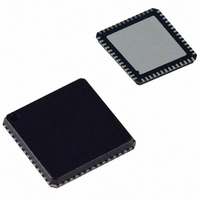
ADUC847BCPZ8-5 Analog Devices Inc, ADUC847BCPZ8-5 Datasheet - Page 13

ADUC847BCPZ8-5
Manufacturer Part Number
ADUC847BCPZ8-5
Description
IC,Data Acquisition CODEC,2-CHANNEL,LLCC,56PIN,PLASTIC
Manufacturer
Analog Devices Inc
Series
MicroConverter® ADuC8xxr
Datasheet
1.EVAL-ADUC845QSZ.pdf
(108 pages)
Specifications of ADUC847BCPZ8-5
Core Processor
8052
Core Size
8-Bit
Speed
12.58MHz
Connectivity
I²C, SPI, UART/USART
Peripherals
POR, PSM, PWM, Temp Sensor, WDT
Number Of I /o
34
Program Memory Size
8KB (8K x 8)
Program Memory Type
FLASH
Eeprom Size
4K x 8
Ram Size
2.25K x 8
Voltage - Supply (vcc/vdd)
4.75 V ~ 5.25 V
Data Converters
A/D 10x24b; D/A 1x12b, 2x16b
Oscillator Type
Internal
Operating Temperature
-40°C ~ 85°C
Package / Case
56-LFCSP
Lead Free Status / RoHS Status
Lead free / RoHS Compliant
For Use With
EVAL-ADUC847QSZ - KIT DEV QUICK START FOR ADUC847
Lead Free Status / RoHS Status
Lead free / RoHS Compliant
Pin No:
52-MQFP
20, 34, 48
21, 35, 47
26
27
28–31,
36–
28
29
30
31
36
37
38
39
32
33
40
41
42
39
Pin No: 56-
LFCSP
22, 36, 51
23, 3
28
29
30–33, 39–
42
30
31
32
33
39
40
41
42
34
35
43
44
45
7, 38, 50
Mnemonic
DV
DGND
SCLK (I
SDATA
P2.0–P2.7
P2.0/SCLOCK (SPI)
P2.1/MOSI
P2.2/MISO
P2.3/SS/T2
P2.4/T2EX
P2.5/PWM0
P2.6/PWM1
P2.7/PWMCLK
XTAL1
XTAL2
EA
PSEN
ALE
DD
2
C)
Type
S
S
I/O
I/O
I/O
I
O
O
O
1
Rev. B | Page 13 of 108
Description
Digital Supply Voltage.
Digital Ground.
Serial Interface Clock for the I
triggered input. A weak
outputting logic
output pin.
Serial Data Pin for the I
pull-up present unless it is outputting logic low.
Port 2 is a bid
have 1s written to them are pulled high by the internal pull-up resistors, and
in that state can be used as inputs. As inputs, Port
externally low source current because of the internal pull-up resistors. Port 2
emits the middle and high-order address bytes during accesses to the 24-bit
external data memory space.
Port 2 pins also have the various secondary functions described below.
Serial Interface Clock for the SPI Interface. As an input this pin is a Schmitt-
triggered input. A weak interna
outputting logic low.
Serial Master Output/Slave Input Data for the SPI Interface. A strong interna
pull-up is present on this pin when the SPI interface outputs a logic high.
strong internal pull-do
outputs a logic low.
Master Input/Slave Output for the SPI Interface. A weak pull-up is present on
this input pin.
Slave Select Input for the SPI
For both package options, this pin can also be used to provide a clock input to
Timer 2. When e
transition on the T2 input pin.
Control Input to Timer 2. When enabled, a negative transition on the T2EX
input pin causes a Timer 2 capture or reload event.
If the PWM is enabled, the PWM
If the PWM is enabled, the PWM1 output appears at this pin.
If the PWM is enabled, an external PWM clock can be
Input to the Crystal Oscillator Inverter.
Output from the Crystal Oscillator Inverter. See the Hardware Desig
Considerations section for a description.
External Access Enable, Logic Input. When held high, this input enables the
device to fetch code from internal program memory locations 0000H
F7FFH. No external program memory acce
ADuC847, or ADuC848. To determine the mode of code execution, the EA pin
is sampled at the end of an external RESET assertion or as part of a device
power cycle. EA can also be used as an external emulation I/O pin, and
therefore the voltage level at this pin must not be changed during normal
operation because this might cause an emulation interrupt that halts code
execution.
Program Store Enable, Logic Output. This function is not used on the
ADuC845, ADuC847, or ADuC848. This pin remains high during internal
program exe
PSEN can also be used to enable serial download mode when pulled lo
through a resistor at the end of an external RESET assertion or as part o
device power cycle.
Address Latch Enable, Logic Output. This output is used to latch the low by
(and page byte for 24-bit data address space accesses) of the address to
external memory dur
disabled by setting the PCON.4 bit in the PCON SFR.
cution.
irectional port with internal pull-up resistors. Port 2 pins that
nabled, Counter 2 is incremented in response to a negative
low. This pin can also be controlled in software as a digital
ing external data memory access cycles. It can be
2
wn is present on this pin when the SPI interface
C Interface. As an input, this pin has a weak intern
internal pull-up is present on this pin unless it is
Interface. A weak pull-up is present on this pin.
2
C Interface. As an input, this pin is a Schmitt-
l pull-up is present on this pin unless it is
0 output appears at this pin.
ADuC845/ADuC847/ADuC848
ss is available on the ADuC845,
2 pins being pulled
provided at this pin.
n
to
w
f a
al
A
te
l


