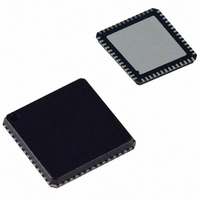
ADUC847BCPZ8-5 Analog Devices Inc, ADUC847BCPZ8-5 Datasheet - Page 30

ADUC847BCPZ8-5
Manufacturer Part Number
ADUC847BCPZ8-5
Description
IC,Data Acquisition CODEC,2-CHANNEL,LLCC,56PIN,PLASTIC
Manufacturer
Analog Devices Inc
Series
MicroConverter® ADuC8xxr
Datasheet
1.EVAL-ADUC845QSZ.pdf
(108 pages)
Specifications of ADUC847BCPZ8-5
Core Processor
8052
Core Size
8-Bit
Speed
12.58MHz
Connectivity
I²C, SPI, UART/USART
Peripherals
POR, PSM, PWM, Temp Sensor, WDT
Number Of I /o
34
Program Memory Size
8KB (8K x 8)
Program Memory Type
FLASH
Eeprom Size
4K x 8
Ram Size
2.25K x 8
Voltage - Supply (vcc/vdd)
4.75 V ~ 5.25 V
Data Converters
A/D 10x24b; D/A 1x12b, 2x16b
Oscillator Type
Internal
Operating Temperature
-40°C ~ 85°C
Package / Case
56-LFCSP
Lead Free Status / RoHS Status
Lead free / RoHS Compliant
For Use With
EVAL-ADUC847QSZ - KIT DEV QUICK START FOR ADUC847
Lead Free Status / RoHS Status
Lead free / RoHS Compliant
ADuC845/ADuC847/ADuC848
Signal Chain Overview with Chop Disabled (CHOP = 1)
With CHOP = 1, chop is disabled and the available output rates
vary from 16.06 Hz to 1.365 kHz. The range of applicable SF
words is from 3 to 255. When switching between channels with
chop disabled, the channel throughput rate is higher than wh
chop is enabled. The drawback with chop disabled is that the
drift performance is degraded and offset calibration is require
following a gain range change or significant temperature
change. A block diagram of the ADC input channel with chop
disable
The signal chain includes a multiplex or buffer, PGA, Σ-Δ
modulator, and digital filter. The modulator bit stream is
applied to a Sinc
fa
factor is the register value times 8. The decimated output rate
from the Sinc filter (and the ADC conversion rate) is therefore
wher
f
SF is
regis
f
ADC
MO
ctor is restricted to an 8-bit register SF; the actual decimation
D
is the AD
is the modulator sampling rate of 32.768 kHz.
ter, valid ran
e:
the deci
f
ADC
d is shown in Figure 15.
=
mal eq
8
3
C con
×
1
3
SF
ge is f
filter. Programming the Sinc
version rate.
×
uivalent of th
f
MOD
rom 3 to 255.
ANALOG
INPUT
e word
MUX
loade
Figure 15. Block Diagram of ADC Input Channel with Chop Disabled
d to th
3
BUF
decimation
e filter
PGA
F
IN
Rev. B | Page 30 of 108
en
d
F
MOD
Σ-∆
MOD
The settling time to a step input is governed by the digital filte
A synchronized step change requires a settling time of three
times the programmed update rate; a channel change can be
treated as a synchronized step change. This is one conversion
longer than the case for chop enabled. However, be
ADC throughput is three times faster with chop disabled than it
is with chop enabled, the actual time to a settled ADC output is
significantly less also. This means that following a synchronized
step change, the ADC requires three conversions (note: data is
not output following a synchronized ADC change until data h
settled) before the result accurately reflects the new input
voltage.
An unsynchronized step change requires four conversions to
accur
with an u ynchronize
data a
Aga
bec
with
AD
The allowable range for SF is 3 to 255 with a default of 69 (45H).
The corresponding conversion rates, rms, and peak-to-peak
noise
and Tabl
for each
SINC
ause the
C outpu
in, this is one conversion longer tha
3
chop e
t
ately reflect th
performances
SETTLE
nd so
FILTER
e 1
incr
ns
7. Note that
nable
t is le
the user
ADC
em
=
ent in
f
ADC
ss.
d, the ac
3
through
8 × SF
e new analog input at its output. Note that
are shown in Table 14, Table 15, Table 16,
mus
=
SF.
d c
F
th
3
ADC
×
t take un
e conversio
tual ti
put w
hange the
t
ADC
DIGITAL
OUTPUT
ith chop
me take
settle
AD
n ti
d output
n to o
n with
me incre
disa
C contin
bled is f
btain a
chop
s int
ases
ues
cause the
aster
o accoun
enable
to outpu
sett
by 0.244
led
than
d, but
t.
t
ms
as
r.


