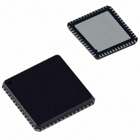
ADUC847BCPZ8-5 Analog Devices Inc, ADUC847BCPZ8-5 Datasheet - Page 64

ADUC847BCPZ8-5
Manufacturer Part Number
ADUC847BCPZ8-5
Description
IC,Data Acquisition CODEC,2-CHANNEL,LLCC,56PIN,PLASTIC
Manufacturer
Analog Devices Inc
Series
MicroConverter® ADuC8xxr
Datasheet
1.EVAL-ADUC845QSZ.pdf
(108 pages)
Specifications of ADUC847BCPZ8-5
Core Processor
8052
Core Size
8-Bit
Speed
12.58MHz
Connectivity
I²C, SPI, UART/USART
Peripherals
POR, PSM, PWM, Temp Sensor, WDT
Number Of I /o
34
Program Memory Size
8KB (8K x 8)
Program Memory Type
FLASH
Eeprom Size
4K x 8
Ram Size
2.25K x 8
Voltage - Supply (vcc/vdd)
4.75 V ~ 5.25 V
Data Converters
A/D 10x24b; D/A 1x12b, 2x16b
Oscillator Type
Internal
Operating Temperature
-40°C ~ 85°C
Package / Case
56-LFCSP
Lead Free Status / RoHS Status
Lead free / RoHS Compliant
For Use With
EVAL-ADUC847QSZ - KIT DEV QUICK START FOR ADUC847
Lead Free Status / RoHS Status
Lead free / RoHS Compliant
ADuC845/ADuC847/ADuC848
SPI SERIAL INTERFACE
The ADuC845/ADuC847/ADuC848 integrate a complete
hardware serial peripheral interface (SPI) interface on-chip. SPI
is an industry-standard synchronous serial interface that allows
8 bits of data to be synchronously transmitted and received
simultaneously, that is, full duplex. Note that the SPI pins are
multiplexed with the Port 2 pins, P2.0, P2.1, P2.2, and P2.3. These
pins have SPI functionality only if SPE is set. Otherwise, with
SPE cleared, standard Port 2 functionality is maintained. SPI
can be configured for master or slave operation and typically
consists of Pins SCLOCK, MISO, MOSI, and SS .
SCLOCK (Serial Clock I/O Pin)
Pin 28 (MQFP Package), Pin 30 (LFCSP Package)
The master clock (SCLOCK) is used to synchronize the data
transmitted and received through the MOSI and MISO data
lines.
A single data bit is transmitted and received in each SCLOCK
period. Therefore, a byte is transmitted/received after eight
SCLOCK periods. The SCLOCK pin is configured as an output
in master mode and as an input in slave mode. In master mode,
the bit rate, polarity, and phase of the clock are controlled by the
CPOL, CPHA, SPR0, and SPR1 bits in the SPICON SFR (see
Table 41). In slave mode, the SPICON register must be config-
ured with the same phase and polarity (CPHA and CPOL) as the
master. The data is transmitted on one edge of the SCLOCK
signal and sampled on the other.
Rev. B | Page 64 of 108
MISO (Master In, Slave Out Pin)
Pin 30 (MQFP Package), Pin 32 (LFCSP Package)
The MISO pin is configured as an input line in master mode
and an output line in slave mode. The MISO line on the master
(data in) should be connected to the MISO line in the slave
device (data out). The data is transferred as byte-wide (8-bit)
serial data, MSB first.
MOSI (Master Out, Slave In Pin)
Pin 29 (MQFP Package), Pin31 (LFCSP Package)
The MOSI pin is configured as an output line in master mode
and an input line in slave mode. The MOSI line on the master
(data out) should be connected to the MOSI line in the slave
device (data in). The data is transferred as byte-wide (8-bit)
serial data, MSB first.
SS (Slave Select Input Pin)
Pin 31 (MQFP Package), Pin 33 (LFCSP Package)
The SS pin is used only when the ADuC845/ADuC847/
ADuC848 are configured in SPI slave mode. This line is active
low. Data is received or transmitted in slave mode only when
the SS pin is low, allowing the parts to be used in single-master,
multislave SPI configurations. If CPHA = 1, the SS input can be
pulled low permanently. If CPHA = 0, the SS input must be
driven low before the first bit in a byte-wide transmission or
reception and must return high again after the last bit in that
byte-wide transmission or reception. In SPI slave mode, the
logic level on the external SS pin (Pin 31/Pin 33) can be read via
the SPR0 bit in the SPICON SFR.
The SFR register in Table 41 is used to control the SPI interface.


