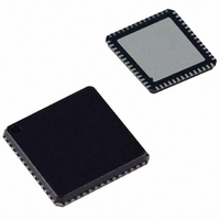
ADUC847BCPZ8-5 Analog Devices Inc, ADUC847BCPZ8-5 Datasheet - Page 32

ADUC847BCPZ8-5
Manufacturer Part Number
ADUC847BCPZ8-5
Description
IC,Data Acquisition CODEC,2-CHANNEL,LLCC,56PIN,PLASTIC
Manufacturer
Analog Devices Inc
Series
MicroConverter® ADuC8xxr
Datasheet
1.EVAL-ADUC845QSZ.pdf
(108 pages)
Specifications of ADUC847BCPZ8-5
Core Processor
8052
Core Size
8-Bit
Speed
12.58MHz
Connectivity
I²C, SPI, UART/USART
Peripherals
POR, PSM, PWM, Temp Sensor, WDT
Number Of I /o
34
Program Memory Size
8KB (8K x 8)
Program Memory Type
FLASH
Eeprom Size
4K x 8
Ram Size
2.25K x 8
Voltage - Supply (vcc/vdd)
4.75 V ~ 5.25 V
Data Converters
A/D 10x24b; D/A 1x12b, 2x16b
Oscillator Type
Internal
Operating Temperature
-40°C ~ 85°C
Package / Case
56-LFCSP
Lead Free Status / RoHS Status
Lead free / RoHS Compliant
For Use With
EVAL-ADUC847QSZ - KIT DEV QUICK START FOR ADUC847
Lead Free Status / RoHS Status
Lead free / RoHS Compliant
ADuC845/ADuC847/ADuC848
AUXILIARY ADC (ADUC845 ONLY)
Table 18. ADuC845 Typical Output RMS Noise (µV) vs.
Update Rate with Chop Enabled
SF Word
13
23
27
69
255
Table 19. ADuC845 Typical Peak-to-Peak Resolution (Bits)
Update Rate
SF Word
13
23
27
69
255
1
Table 20. ADuC845 Typical Output RMS Noise (µV) vs.
Update Rate with Chop Disabled
SF Word
3
13
66
69
81
255
Table 21. ADuC845 Peak-to-Peak Resolution (Bits) vs.
Update Rate with Chop Disabled
SF Word
3
13
66
69
81
255
REFERENCE INPUTS
The ADuC845/ADuC847/ADuC848 each have two separate
differential reference inputs, REFIN± and REFIN2±. While
both references are available for use with the primary ADC,
only REFIN± is available for the auxiliary ADC (ADuC845
only). The common-mode range for these differential
references is from AGND to AV
reference voltage is 2.5 V, with the primary and auxiliary
(ADuC845 only) reference select bits configured from the
ADC0CON2 and ADC1CON (ADuC845 only), respectively.
ADC converting in bipolar mode.
Data Update Rate (Hz)
1365.33
315.08
62.06
59.36
50.57
16.06
1
Data Update Rate (Hz)
1365.33
315.08
62.06
59.36
50.57
16.06
with Chop Enabled
105.03
59.36
50.56
19.79
5.35
105.03
59.36
50.56
19.79
5.35
Data Update Rate (Hz)
Data Update Rate (Hz)
DD
. The nominal external
µV
17.46
3.13
4.56
2.66
1.13
Bits
15.5
18
17.5
18
19.5
µV
1386.58
34.94
3.2
3.19
3.14
1.71
Bits
9
14.5
18
18
18
19
Rev. B | Page 32 of 108
vs.
When an external reference voltage is used, the primary ADC
sees this internally as a 2.56 V reference (V
Therefore, any calculat
For instance, with a 2.5
using a gain of 1 on a unipolar range (2.56 V), the LSB size i
(2.56/2
or ADuC847). If a bipolar gain of 4 is used (±640 mV), th
size is (±640 mV)/2
on the ADuC845 or ADuC84
The ADuC845/ADuC847/ADuC848 can also be configured to
use the on-chip band gap reference via the XREF0/1 bits in the
ADC0CON2 SFR (for primary ADC) or the AXREF bit in
ADC1CON (for auxiliary ADC (ADuC845 only)). In this mode
of operation, the ADC sees the internal reference of 1.25 V,
thereby halving all the input ranges. A consequence of using th
internal ba
to-peak resolution. For this reason, operation with an external
reference is recommended.
In applications where the excitation (voltage or current) for the
transducer on the analog input also drives the reference inputs
for the part, the effect of any low frequency noise in the
excitation source is removed because the application is ratio-
metric. If the parts are not used in a ratiometric configuratio
low noise reference should be used. Recommended reference
voltage sources for the ADuC845/ADuC847/ADuC848 include
ADR421, REF43, and REF192.
The reference inputs provide a high impedance, dynamic
to external connections. Because the impedance of each refer
input is dynamic, resistor/capacitor combinations on these pins
can cause dc gain errors, dep
the source that is driv
sources, such as those me
ADR421, typically have low output impedances, and, therefore,
decoupling capacitors on the REFIN± or REFIN2± inputs w
be recommended (typically 0.1 µF). Deriving the reference
voltage from an external resistor configuration means that the
reference input sees a significant external source impedance.
External decoupling of the REFIN± and/or REFIN2± inputs is
not recommended in this type of configuration.
BURNOUT CURRENT SOURCES
The primary ADC on the ADuC845 and the ADC on the
ADuC847 and ADuC848 incorporate two 200 µA constant
current genera
connected sensor. One sources current from the AV
AIN(+), and one sinks current from AIN(−) to AGND. These
currents are only configurable for use on AIN5/AIN6 and/or
AIN7/AIN8 in differential mode only, from the ICON.6 bit in
the ICON SFR (see Table 30). These burnout current sources
are also available only with buffering enabled via the BUF0/BUF1
bits in the ADC0CON1 SFR. Once the burnout currents are
turned on, a current flows in the external transducer circuit,
24
) = 152.6 nV (if using the 24-bit ADC on the ADuC8
nd gap reference is a noticeable degradation
tors that are used to detect a failure in a
24
) = 76.3 nV (again using the 24-bit ADC
ing the reference inputs. Reference voltage
ions of LSB size should account for this.
V external reference connected and
ntioned above, for example, the
ending on the output impedance of
7).
REF
× 1.024).
DD
to
in peak-
e LSB
load
ould
ence
s
n, a
45
e


