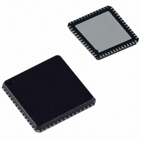
ADUC847BCPZ8-5 Analog Devices Inc, ADUC847BCPZ8-5 Datasheet - Page 62

ADUC847BCPZ8-5
Manufacturer Part Number
ADUC847BCPZ8-5
Description
IC,Data Acquisition CODEC,2-CHANNEL,LLCC,56PIN,PLASTIC
Manufacturer
Analog Devices Inc
Series
MicroConverter® ADuC8xxr
Datasheet
1.EVAL-ADUC845QSZ.pdf
(108 pages)
Specifications of ADUC847BCPZ8-5
Core Processor
8052
Core Size
8-Bit
Speed
12.58MHz
Connectivity
I²C, SPI, UART/USART
Peripherals
POR, PSM, PWM, Temp Sensor, WDT
Number Of I /o
34
Program Memory Size
8KB (8K x 8)
Program Memory Type
FLASH
Eeprom Size
4K x 8
Ram Size
2.25K x 8
Voltage - Supply (vcc/vdd)
4.75 V ~ 5.25 V
Data Converters
A/D 10x24b; D/A 1x12b, 2x16b
Oscillator Type
Internal
Operating Temperature
-40°C ~ 85°C
Package / Case
56-LFCSP
Lead Free Status / RoHS Status
Lead free / RoHS Compliant
For Use With
EVAL-ADUC847QSZ - KIT DEV QUICK START FOR ADUC847
Lead Free Status / RoHS Status
Lead free / RoHS Compliant
ADuC845/ADuC847/ADuC848
I2CADD—I
Function:
SFR Address:
Power-On Default:
Bit Addressable:
I2CADD1—I
Function:
SFR Address:
Power-On Default:
Bit Addressable:
I2CDAT—I
Function:
SFR Address:
Power-On Default:
Bit Addressable:
The main features of the MicroConverter I
•
•
•
•
Only two bus lines are required: a serial data line (SDATA)
and a serial clock line (SCLOCK).
An I
devices. Because each slave device has a unique 7-bit
address, single master/slave relationships can exist at all
times even in a multislave environment.
The ability to respond to two separate addresses when
operating in slave mode.
On-chip filtering rejects <50 ns spikes on the SDATA and
the SCLOCK lines to preserve data integrity.
2
C master can communicate with multiple slave
2
2
C Data Register
C Address Register 1
2
C Address Register 2
MASTER
I
2
C
Figure 45. Typical I
Holds one of the I
Note uC001 at
9BH
55H
No
Same as the I2CADD.
F2H
7FH
No
The I2CDAT SFR is written to by user code to transmit data, or read by user code to read data just received by
the I
I2CCON SFR. User code should access I2CDAT only once per interrupt cycle.
9AH
00H
No
DV
2
DD
C interface. Accessing I2CDAT automatically clears any pending I
2
C System
SLAVE 1
SLAVE 2
http://www.analog.com/microconverter
I
I
2
2
C
C
2
2
C interface are
C peripheral addresses for the part. It may be overwritten by user code. Application
Rev. B | Page 62 of 108
Software Master Mode
The ADuC845/ADuC847/ADuC848 can be used as an I
master device by configuring the I
and writing software to output the data bit-by-bit. This is
referred to as a software master. Master mode is enabled by
setting the I2CM bit in the I2CCON register.
To transmit data on the SDATA line, MDE must be set to enable
the output driver on the SDATA pin. If MDE is set, the SDATA
pin is pulled high or low depending on whether the MDO bit is
set or cleared. MCO controls the SCLOCK pin and is always
configured as an output in master mode. In master mode, the
SCLOCK pin is pulled high or low depending on the whether
MCO is set or cleared.
To receive data, MDE must be cleared to disable the output
driver on SDATA. Software must provide the clocks by toggling
the MCO bit and reading the SDATA pin via the MDI bit. If
MDE is cleared, MDI can be used to read the SDATA pin. The
value of the SDATA pin is latched into MDI on a rising edge of
SCLOCK. MDI is set if the SDATA pin is high on the last rising
edge of SCLOCK. MDI is cleared if the SDATA pin is low on the
last rising edge of SCLOCK.
Software must control MDO, MCO, and MDE appropriately to
generate the start condition, slave address, acknowledge bits,
data bytes, and stop conditions. These functions are described
in Application Note uC001.
describes the format of the I
2
C interrupt and the I2CI bit in the
2
C peripheral in master mode
2
C standard 7-bit address.
2
C


