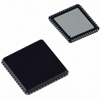
ADUC847BCPZ8-5 Analog Devices Inc, ADUC847BCPZ8-5 Datasheet - Page 35

ADUC847BCPZ8-5
Manufacturer Part Number
ADUC847BCPZ8-5
Description
IC,Data Acquisition CODEC,2-CHANNEL,LLCC,56PIN,PLASTIC
Manufacturer
Analog Devices Inc
Series
MicroConverter® ADuC8xxr
Datasheet
1.EVAL-ADUC845QSZ.pdf
(108 pages)
Specifications of ADUC847BCPZ8-5
Core Processor
8052
Core Size
8-Bit
Speed
12.58MHz
Connectivity
I²C, SPI, UART/USART
Peripherals
POR, PSM, PWM, Temp Sensor, WDT
Number Of I /o
34
Program Memory Size
8KB (8K x 8)
Program Memory Type
FLASH
Eeprom Size
4K x 8
Ram Size
2.25K x 8
Voltage - Supply (vcc/vdd)
4.75 V ~ 5.25 V
Data Converters
A/D 10x24b; D/A 1x12b, 2x16b
Oscillator Type
Internal
Operating Temperature
-40°C ~ 85°C
Package / Case
56-LFCSP
Lead Free Status / RoHS Status
Lead free / RoHS Compliant
For Use With
EVAL-ADUC847QSZ - KIT DEV QUICK START FOR ADUC847
Lead Free Status / RoHS Status
Lead free / RoHS Compliant
Therefore, the full-scale endpo
subtracts the offset calibration error, it is advisable to perform
an offset calibration at the same gain range as that used for full-
scale calibration. There is no penalty to the full-scale calibration
in redoing the zero-scale calibration at the required PGA range
because the full-scale calibration has very good matching at all
the PGA ranges.
This p
Note th
should b
mode range to keep it from floatin
System Calibration Example
With chop enabled, a system zero-scale or offset calibration
should never be required. However, if a full-scale or gain
calibration is required for any reason, use the following typica
procedure for doing so.
1.
2.
Perform
used since the ADC scales to the
applied to the ADC during the calibration routines.
In bipolar mode, the zero-scale
scale point of the ADC (800000
PROGRAMMABLE GAIN AMPLIFIER
The primary ADC incorporates an on-chip programmable gain
amp
different ranges, which are prog mmed via the range bits (RN0
t
re
to 40 mV, 0 mV to 80 mV, 0 mV to 160 mV, 0 mV to 320 mV,
0 mV to 640 mV, 0 V to 1.28 V and 0 V to 2.56 V, while in
bipolar mode the ranges are ±20 mV, ±40 mV, ±80 mV, ±160 mV,
±320 mV, ±64 0 mV, ±1.28 V, and ±2.56 V. These ranges should
appear on the input to the on-chip PGA. The ADC range-
matching specification of 2 µV (typical with chop enabled)
means that calibration need only be carried out on a single
range and need not be repeated when the ADC range is
changed. This is a significant advantage compared to similar
o RN2) in the ADC0CON1 register. With an external 2.5 V
ference applied, the unipolar ranges are 0 mV to 20 mV, 0 mV
lifier (PGA). The PGA can be p
Apply a different al voltag
inputs (AIN+ to AIN−) that are held at a common-mode
voltage.
Perform a system zero-scale or offset calibration by setting
the MD2...0 bits in the ADCMODE register to 110B.
Apply a full-scale differential voltage across the ADC
inputs again at the same common-mode voltage.
Perform a system full-scale or gain cal ration b
the MD2
rocedure also applies when chop is dis bl
at for internal calibration to be effective, the AIN− pin
e held at a steady voltage, within the allowable common-
a system calibration at the required PGA range to be
...0 b
its in the ADCMODE register to 1
i
e of 0 V to the selected analog
int calibration automatically
H) or 0 V.
calibration determines the mid-
ra
differential voltages that are
g during calibration.
rogrammed through eight
ib
a ed.
11B.
y setting
Rev. B | Page 35 of 108
l
mixed-signal solutions availabl
(ADuC845 only) ADC does not incorporate a PGA, and the
gain is fixed at 0 V to 2.50 V in unipolar mode, and ±2.50 V
bipolar mode.
BIPOLAR/UNIPOLAR CONFIGURATION
The analog inputs of the ADuC845/ADuC847/ADuC848 can
accept either unipolar or bipolar input voltage ranges. Bipolar
input ranges do not imply that the part can handle negative
voltages with respect to system AGND, but rather with respec
to the negative reference input. Unipolar and bipolar signals on
the AIN(+) input on the ADC are referenced to the voltage on
the respective AIN(−) input. AIN(+) and AIN(−) refer to the
signals seen by the ADC.
For example, if AIN(−) is biased to 2.5 V (tied to the external
reference voltage) and the ADC is configured for a unipolar
analog input range of 0 mV to >20 mV, the input volta
on AIN(+) is 2.5 V to 2.52 V. O
biased to 2.5 V (again the external reference voltage) and the
ADC is configured for a bipolar analog input range of ±1.28 V,
the analog input range on the AIN(+) is 1.22 V to 3.78 V, that is,
2.5 V ± 1.28 V.
The modes of operation for the ADC are fully differential mode
or pseudo differential mode. In fully differential mode, AIN1 to
AIN2 are one differential pair, and AIN3 to AIN4 are another
pair (AIN5 to AIN6, AIN7 to AIN8, and AIN9 to AIN10 are the
others). In differential mode, all AIN(−) pin names imply the
negative analog input of the selected differential pair, that is,
AIN2, AIN4, AIN6, AIN8, AIN10. The term AIN(+) implies
the positive input of the selected differential pair, that is, AIN1,
AIN3, AIN5, AIN7, AIN9. In pseudo differential mode, each
analog input is paired with the AINCOM pin, which can be
biased up or tied to AGND. In this mode, the AIN(−) implies
AINCOM, and AIN(+) implies any one of the ten analog input
channels.
The configuration of the inputs (unipolar vs. bipolar) is shown
in Figure 17.
Figure 17. Unipolar and Bipolar Channel Pairs
ADuC845/ADuC847/ADuC848
AIN1
AIN2
AIN3
AIN4
AIN5
AIN6
AIN7
AIN8
AIN9
AIN10
AINCOM
e on the market. The auxiliary
n t
FULLY DIFFERENTIAL
FULLY DIFFERENTIAL
FULLY DIFFERENTIAL
FULLY DIFFERENTIAL
FULLY DIFFERENTIAL
he other hand, if AIN(−) is
AIN1
AIN2
AIN3
AIN4
AIN5
AIN6
AIN7
AIN8
AIN9
AIN10
AINCOM
ge range
in
t


