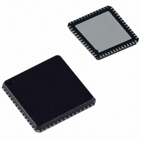
ADUC847BCPZ8-5 Analog Devices Inc, ADUC847BCPZ8-5 Datasheet - Page 9

ADUC847BCPZ8-5
Manufacturer Part Number
ADUC847BCPZ8-5
Description
IC,Data Acquisition CODEC,2-CHANNEL,LLCC,56PIN,PLASTIC
Manufacturer
Analog Devices Inc
Series
MicroConverter® ADuC8xxr
Datasheet
1.EVAL-ADUC845QSZ.pdf
(108 pages)
Specifications of ADUC847BCPZ8-5
Core Processor
8052
Core Size
8-Bit
Speed
12.58MHz
Connectivity
I²C, SPI, UART/USART
Peripherals
POR, PSM, PWM, Temp Sensor, WDT
Number Of I /o
34
Program Memory Size
8KB (8K x 8)
Program Memory Type
FLASH
Eeprom Size
4K x 8
Ram Size
2.25K x 8
Voltage - Supply (vcc/vdd)
4.75 V ~ 5.25 V
Data Converters
A/D 10x24b; D/A 1x12b, 2x16b
Oscillator Type
Internal
Operating Temperature
-40°C ~ 85°C
Package / Case
56-LFCSP
Lead Free Status / RoHS Status
Lead free / RoHS Compliant
For Use With
EVAL-ADUC847QSZ - KIT DEV QUICK START FOR ADUC847
Lead Free Status / RoHS Status
Lead free / RoHS Compliant
Parameter
1
2
3
4
5
6
7
8
9
10
11
Normal mode: reset = 0.4 V, digital I/O pins = open circuit, Core Clk changed via CD bits in PLLCON, core executing internal software loop.
Power-down mode: reset = 0.4 V, all P0 pins and P1.2 to P1.7 pins = 0.4 V. All other digital I/O pins are open circuit, core Clk changed via CD bits in PLLCON, PCON.1 = 1,
12
General Notes about Specifications
•
•
•
Temperature range is for ADuC845BS; for the ADuC847BS and ADuC848BS (MQFP package), the range is –40°C to +125°C.
These numbers are not production tested but are guaranteed by design and/or characterization data on production release.
System zero-scale calibration can remove this error.
Gain error drift is a span drift. To calculate full-scale error drift, add the offset error drift to the gain error drift times the full-scale input.
In general terms, the bipolar input voltage range to the primary ADC is given by the ADC range = ±(V
RN1, RN0 = 1, 1, 0, respectively, then the ADC range = ±1.28 V. In unipolar mode, the effective range is 0 V to 1.28 V in this example.
1.25 V is used as the reference voltage to the ADC when internal V
In bipolar mode, the auxiliary ADC can be driven only to a minimum of AGND – 30 mV as indicated by the auxiliary ADC absolute AIN voltage limits. The bipolar range
is still –V
DAC linearity and ac specifications are calculated using a reduced code range of 48 to 4095, 0 V to V
Endurance is qualified to 100 kcycle per JEDEC Std. 22 method A117 and measured at –40°C, +25°C, +85°C, and +125°C. Typical endurance at 25°C is 700 kcycles.
core execution suspended in power-down mode, OSC turned on or off via OSC_PD bit (PLLCON.7) in PLLCON SFR.
Temperature range for ADuC845BCP, ADuC847BCP, and ADuC848BCP (LFCSP package) is –40°C to +85°C.
V
(AXREF is available only on the ADuC845.)
Retention lifetime equivalent at junction temperature (T
Power supply current consumption is measured in normal mode following the power-on sequence, and in power-down modes under the following conditions:
DV
with junction temperature.
REF
3 V Power Consumption
DD
= REFIN(+) to REFIN(–) voltage and V
PWM
TIC
Normal Mode
Power-Down Mode
DAC gain error is a measure of the span error of the DAC.
The ADuC845BCP, ADuC847BCP, and ADuC848BCP (LFCSP package) have been qualified and tested with the base of the LFCSP
package floating. The base of the LFCSP package should be soldered to the board, but left floating electrically, to ensure good
mechanical stability.
Flash/EE memory reliability characteristics apply to both the Flash/EE program memory and Flash/EE data memory.
power supply current increases typically by 3 mA (3 V operation) and 10 mA (5 V operation) during a Flash/EE memory program or erase cycle.
−Fxtal
−Fvco
DV
AV
DV
AV
REF
DD
DD
DD
DD
to +V
Current
Current
Current
Current
REF
.
11, 12
11, 12
REF
= 1.25 V when internal ADC V
Min
J
) = 55°C per JEDEC Std. 22, Method A117. Retention lifetime based on an activation energy of 0.6 eV derates
Typ
3
0.5
1
9
20
29
14
21
REF
is selected via XREF0/XREF1 or AXREF bits in ADC0CON2 and ADC1CON, respectively.
Rev. B | Page 9 of 108
REF
is selected. RN = decimal equivalent of RN2, RN1, RN0. For example, if V
Max
4.8
11
180
26
20
1
3
Unit
mA
µA
mA
mA
µA
µA
µA
µA
µA
µA
µA
µA
REF
REF
, reduced code range of 100 to 3950, 0 V to V
2
RN
)/1.25, where:
Conditions
2.7 V < DV
Core clock = 1.57 MHz
Core clock = 6.29 MHz (CD = 1)
ADC not enabled
T
T
T
T
T
T
MAX
MAX
MAX
MAX
MAX
MAX
ADuC845/ADuC847/ADuC848
= 85°C; OSC on; TIC on
= 125°C; OSC on; TIC on
= 85°C; OSC off
= 125°C; OSC off
= 85°C; OSC on or off
= 125°C; OSC on or off
DD
< 3.6 V, AV
DD
= 3.6 V
REF
DD
.
= 2.5 V and RN2,


