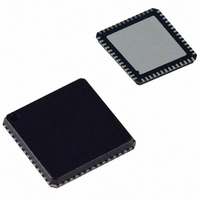
ADUC847BCPZ8-5 Analog Devices Inc, ADUC847BCPZ8-5 Datasheet - Page 51

ADUC847BCPZ8-5
Manufacturer Part Number
ADUC847BCPZ8-5
Description
IC,Data Acquisition CODEC,2-CHANNEL,LLCC,56PIN,PLASTIC
Manufacturer
Analog Devices Inc
Series
MicroConverter® ADuC8xxr
Datasheet
1.EVAL-ADUC845QSZ.pdf
(108 pages)
Specifications of ADUC847BCPZ8-5
Core Processor
8052
Core Size
8-Bit
Speed
12.58MHz
Connectivity
I²C, SPI, UART/USART
Peripherals
POR, PSM, PWM, Temp Sensor, WDT
Number Of I /o
34
Program Memory Size
8KB (8K x 8)
Program Memory Type
FLASH
Eeprom Size
4K x 8
Ram Size
2.25K x 8
Voltage - Supply (vcc/vdd)
4.75 V ~ 5.25 V
Data Converters
A/D 10x24b; D/A 1x12b, 2x16b
Oscillator Type
Internal
Operating Temperature
-40°C ~ 85°C
Package / Case
56-LFCSP
Lead Free Status / RoHS Status
Lead free / RoHS Compliant
For Use With
EVAL-ADUC847QSZ - KIT DEV QUICK START FOR ADUC847
Lead Free Status / RoHS Status
Lead free / RoHS Compliant
USING FLASH/EE DATA MEMORY
The 4 kbytes of Flash/EE data memory are configured as 1024
pages, each of 4 bytes. As with the other ADuC845/ADuC847/
ADuC848 peripherals, the interface to this memory space is via
a group of registers mapped in the SFR space. A group of four
data registers (EDATA1–4) holds the 4 bytes of data at each
page. The page is addressed via the EADRH and EADRL
registers. Finally, ECON is an 8-bit control register that can be
written to with one of nine Flash/EE memory access commands
to trigger various read, write, erase, and verify functions. A
block diagram of the SFR interface to the Flash/EE data memory
array is shown in Figure 32.
ECON—Flash/EE Memory Control SFR
Programming either Flash/EE data memory or Flash/EE
program memory is done through the Flash/EE memory
control SFR (ECON). This SFR allows the user to read, write,
erase, or verify the 4 kbytes of Flash/EE data memory or the
56 kbytes of Flash/EE program memory.
Table 32. ECON—Flash/EE Memory Commands
ECON Value
01H Read
02H Write
03H
04H Verify
05H Erase Page
06H Erase All
81H ReadByte
82H WriteByte
0FH EXULOAD
F0H ULOAD
4 bytes in the Flash/EE data memory, addressed by the
page address EADRH/L, are read into EDATA1–4.
Results in 4 bytes in EDATA1–4 being written to the
Flash/EE data memory, at the page address given by
EADRH (0 ≤ EADRH < 0400H). Note that the 4 bytes in the
page being addressed must be pre-erased.
Reserved.
Verifies that the data in EDATA1–4 is contained in the
page address given by EADRH/L. A subsequent read of
the ECON SFR results in a 0 being read if the verification
is valid, or a nonzero value being read to indicate an
invalid verification.
4-byte page of Flash/EE data memory address is erased
by the page address EADRH/L.
4 kbytes of Flash/EE data memory are erased.
The byte in the Flash/EE data memory, addressed by the
byte address EADRH/L, is read into EDATA1 (0 ≤ EADRH/L
≤ 0FFFH).
The byte in EDATA1 is written into Flash/EE data memory
at the byte address EADRH/L.
Configures the ECON instructions (above) to operate on
Flash/EE data memory.
Enters ULOAD mode; subsequent ECON instructions
operate on Flash/EE program memory.
Command Description
(Normal Mode, Power-On Default)
Rev. B | Page 51 of 108
BYTE
ADDRESSES
ARE GIVEN IN
BRACKETS
Not implemented. Use the MOVC instruction.
Bytes 0 to 255 of internal XRAM are written to the 256 bytes of
Flash/EE program memory at the page address given by
EADRH/L (0 ≤ EADRH/L < E0H).
Note that the 256 bytes in the page being addressed must be
pre-erased.
Reserved.
Not implemented. Use the MOVC and MOVX instructions to
verify the Write in software.
64-byte page of FLASH/EE program memory addressed by the
byte address EADRH/L is erased. A new page starts when EADRL
is equal to 00H, 80H, or C0H.
The entire 56 kbytes of ULOAD are erased.
Not implemented. Use the MOVC command.
The byte in EDATA1 is written into Flash/EE program memory at
the byte address EADRH/L (0 ≤ EADRH/L ≤ DFFFH).
Enters normal mode, directing subsequent ECON instructions to
operate on the Flash/EE data memory.
Enables the ECON instructions to operate on the Flash/EE
program memory. ULOAD entry mode.
Command Description
(ULOAD Mode)
3FFH
3FEH
02H
01H
03H
00H
Figure 32. Flash/EE Data Memory Control and Configuration
(0FFCH)
(0FF8H)
(000CH)
(0008H)
(0004H)
(0000H)
BYTE 1
BYTE 1
BYTE 1
BYTE 1
BYTE 1
BYTE 1
ADuC845/ADuC847/ADuC848
(000DH)
(0FFDH)
(0FF9H)
(0009H)
(0005H)
(0001H)
BYTE 2
BYTE 2
BYTE 2
BYTE 2
BYTE 2
BYTE 2
(0FFEH)
(0FFAH)
BYTE 3
(000EH)
(000AH)
(0006H)
(0002H)
BYTE 3
BYTE 3
BYTE 3
BYTE 3
BYTE 3
(0FFBH)
(0FFFH)
(000FH)
(000BH)
BYTE 4
BYTE 4
BYTE 4
(0007H)
BYTE 4
(0003H)
BYTE 4
BYTE 4


