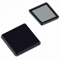
ADUC847BCPZ8-5 Analog Devices Inc, ADUC847BCPZ8-5 Datasheet - Page 89

ADUC847BCPZ8-5
Manufacturer Part Number
ADUC847BCPZ8-5
Description
IC,Data Acquisition CODEC,2-CHANNEL,LLCC,56PIN,PLASTIC
Manufacturer
Analog Devices Inc
Series
MicroConverter® ADuC8xxr
Datasheet
1.EVAL-ADUC845QSZ.pdf
(108 pages)
Specifications of ADUC847BCPZ8-5
Core Processor
8052
Core Size
8-Bit
Speed
12.58MHz
Connectivity
I²C, SPI, UART/USART
Peripherals
POR, PSM, PWM, Temp Sensor, WDT
Number Of I /o
34
Program Memory Size
8KB (8K x 8)
Program Memory Type
FLASH
Eeprom Size
4K x 8
Ram Size
2.25K x 8
Voltage - Supply (vcc/vdd)
4.75 V ~ 5.25 V
Data Converters
A/D 10x24b; D/A 1x12b, 2x16b
Oscillator Type
Internal
Operating Temperature
-40°C ~ 85°C
Package / Case
56-LFCSP
Lead Free Status / RoHS Status
Lead free / RoHS Compliant
For Use With
EVAL-ADUC847QSZ - KIT DEV QUICK START FOR ADUC847
Lead Free Status / RoHS Status
Lead free / RoHS Compliant
•
•
•
•
Wake-Up from Power-Down Latency
Even with the 32 kHz crystal enabled during power-down, the
PLL takes some time to lock after a wake-up from power-down.
Typically, the PLL takes about 1 ms to lock. During this time,
code executes, but not at the specified frequency. Some opera-
tions, for example, UART communications, require an accurate
clock to achieve the specified 50 Hz/60 Hz rejection from the
ADCs. Therefore, it is advisable to wait until the PLL has locked
before proceeding with normal code execution. The following
code can be used to wait for the PLL to lock:
WAITFORLOCK:
If the crystal is powered down during power-down, an additional
delay is associated with the startup of the crystal oscillator
before the PLL can lock. Typically taking about 150 ms, 32 kHz
crystals are inherently slow to oscillate. During this time before
lock, code executes, but the exact frequency of the clock cannot
be guaranteed. For any timing-sensitive operations, it is
recommended to wait for lock by using the lock bit in PLLCON
as previously shown.
An alternative way of saving power in power-down mode
is to slow down the core clock by using the CD bits in the
PLLCON register.
Cycling Power
All registers are set to their default state and program exe-
cution starts at the reset vector approximately 128 ms later.
Time Interval Counter (TIC) Interrupt
If the OSC_PD bit in the PLLCON SFR is clear, the 32 kHz
oscillator remains powered up even in power-down mode.
If the time interval counter (wake-up/RTC timer) is
enabled, a TIC interrupt wakes the part from power-down
mode. The CPU services the TIC interrupt. The RETI at
the end of the TIC ISR returns the core to the next
instruction after that one the enabled power-down.
SPI Interrupt
If the SERIPD bit in the PCON SFR is set, an SPI interrupt,
if enabled, wakes up the part from power-down mode. The
CPU services the SPI interrupt. The RETI at the end of the
ISR returns the core to the next instruction after the one
that enabled power-down.
INT0 Interrupt
If the INT0PD bit in the PCON SFR is set, an external
interrupt 0, if enabled, wakes up the part from power-
down. The CPU services the interrupt. The RETI at the
end of the ISR returns the core to the next instruction after
the one that enabled power-down.
MOV
JNB
A, PLLCON
ACC.6, WAITFORLOCK
Rev. B | Page 89 of 108
GROUNDING AND BOARD LAYOUT
RECOMMENDATIONS
As with all high resolution data converters, special attention
must be paid to grounding and PC board layout of ADuC845/
ADuC847/ADuC848-based designs in order to achieve
optimum performance from the ADCs and DAC.
Although the parts have separate pins for analog and digital
ground (AGND and DGND), the user must not tie these to
separate ground planes unless the two ground planes are
connected together very close to the part as shown in the
simplified example in Figure 68a. In systems where digital and
analog ground planes are connected together somewhere else
(at the system’s power supply, for example), they cannot be
connected again near the part since a ground loop would result.
In these cases, tie the AGND and DGND pins of the part to the
analog ground plane, as shown in Figure 68b. In systems with
only one ground plane, ensure that the digital and analog
components are physically separated onto separate halves of the
board such that digital return currents do not flow near analog
circuitry and vice versa. The parts can then be placed between
the digital and analog sections, as shown in Figure 68c.
In all of these scenarios, and in more complicated real-life
applications, keep in mind the flow of current from the supplies
and back to ground. Make sure that the return paths for all
currents are as close as possible to the paths the currents took to
reach their destinations. For example, do not power
components on the analog side of Figure 68b with DV
that would force return currents from DV
AGND. Also, try to avoid digital currents flowing under analog
circuitry, which could happen if the user placed a noisy digital
chip on the left half of the board in Figure 68c. Whenever
possible, avoid large discontinuities in the ground plane(s)
(such as are formed by a long trace on the same layer), since
they force return signals to travel a longer path. Make all
connections directly to the ground plane, with little or no trace
separating the pin from its via to ground.
ADuC845/ADuC847/ADuC848
DD
to flow through
DD
since


