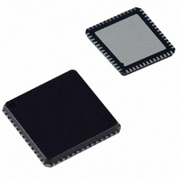
ADUC847BCPZ8-5 Analog Devices Inc, ADUC847BCPZ8-5 Datasheet - Page 87

ADUC847BCPZ8-5
Manufacturer Part Number
ADUC847BCPZ8-5
Description
IC,Data Acquisition CODEC,2-CHANNEL,LLCC,56PIN,PLASTIC
Manufacturer
Analog Devices Inc
Series
MicroConverter® ADuC8xxr
Datasheet
1.EVAL-ADUC845QSZ.pdf
(108 pages)
Specifications of ADUC847BCPZ8-5
Core Processor
8052
Core Size
8-Bit
Speed
12.58MHz
Connectivity
I²C, SPI, UART/USART
Peripherals
POR, PSM, PWM, Temp Sensor, WDT
Number Of I /o
34
Program Memory Size
8KB (8K x 8)
Program Memory Type
FLASH
Eeprom Size
4K x 8
Ram Size
2.25K x 8
Voltage - Supply (vcc/vdd)
4.75 V ~ 5.25 V
Data Converters
A/D 10x24b; D/A 1x12b, 2x16b
Oscillator Type
Internal
Operating Temperature
-40°C ~ 85°C
Package / Case
56-LFCSP
Lead Free Status / RoHS Status
Lead free / RoHS Compliant
For Use With
EVAL-ADUC847QSZ - KIT DEV QUICK START FOR ADUC847
Lead Free Status / RoHS Status
Lead free / RoHS Compliant
HARDWARE DESIGN CONSIDERATIONS
This section outlines some of the key hardware design
considerations that must be addressed when integrating the
ADuC845/ADuC847/ADuC848 into any hardware system.
EXTERNAL MEMORY INTERFACE
In addition to their internal program and data memories, the
parts can access up to 16 Mbytes of external data memory
(SRAM). No external program memory access is available.
To begin executing code, tie the EA (external access) pin high.
When EA is high (pulled up to V
program execution starts at Address 0 in the internal 62-kbyte
Flash/EE code space. When executing from internal code space,
accesses to the program space above F7FFH (62 kbytes) are read
as NOP instructions.
Note that a second very important function of the EA pin is
described in the Single-Pin Emulation Mode section under the
Other Hardware Considerations section.
Figure 62 shows a hardware configuration for accessing up to
64 kbytes of external data memory. This interface is standard to
any 8051-compatible MCU.
If access to more than 64 kbytes of RAM is desired, a feature
unique to the MicroConverter allows addressing up to 16 Mbytes
of external RAM simply by adding another latch as shown in
Figure 63.
Figure 63. External Data Memory Interface (16-Mbtye Address Space)
Figure 62. External Data Memory Interface (64-kbyte Address Space)
ADuC845/
ADuC847/
ADuC848
ADuC845/
ADuC847/
ADuC848
ALE
ALE
WR
WR
RD
RD
P2
P0
P0
P2
LATCH
LATCH
LATCH
DD
—see Figure 70), user
D0–D7
(DATA)
A0–A7
A8–A15
OE
WE
D0–D7
(DATA)
A0–A7
A8–A15
A16–A23
OE
WE
SRAM
SRAM
Rev. B | Page 87 of 108
In either implementation, Port 0 (P0) serves as a multiplexed
address/data bus. It emits the low byte of the data pointer (DPL)
as an address, which is latched by ALE prior to data being placed
on the bus by the parts (write operation) or the external data
memory (read operation). Port 2 (P2) provides the data pointer
page byte (DPP) to be latched by ALE, followed by the data
pointer high byte (DPH). If no latch is connected to P2, DPP is
ignored by the SRAM, and the 8051 standard of 64-kbyte external
data memory access is maintained.
The following example shows the code used to write data to
external data memory.
POWER SUPPLIES
The parts’ operational power supply voltage range is 2.7 V to
5.25 V. Although the guaranteed data sheet specifications are
given only for power supplies within 2.7 V to 3.6 V and 4.75 V
to 5.25 V (±5% of the nominal 5 V level), the chip functions
equally well at any power supply level between 2.7 V and 5.25 V.
Separate analog and digital power supply pins (AV
respectively) allow AV
digital signals often present on a system DV
the part can also operate with split supplies, that is, using different
voltage supply levels for each supply. For example, the system
can be designed to operate with a DV
the AV
split-supply configuration is shown in Figure 64.
As an alternative to providing two separate power supplies,
AV
ferrite bead between it and DV
separately to ground. An example of this configuration is shown
in Figure 65. In this configuration, other analog circuitry (such
DD
MOV DPP, #10h ;Set addr to 100000h
MOV DPH, #00h
MOV DPL, #00h
MOV A,
MOVX @DPTR,A
DIGITAL SUPPLY
can be kept quiet by placing a small series resistor and/or
DD
+
–
0.1µF
level can be at 5 V, or vice versa, if required. A typical
Figure 64. External Dual-Supply Connections
10µF
#'B' ;Write Char ‘B’ (42h)
(56-Lead LFCSP Pin Numbering)
ADuC845/ADuC847/ADuC848
DD
22
36
51
23
37
38
50
to be kept relatively free of the noisy
;Move to DPP:DPH:DPL addr
DGND
DV
DD
ADuC845/
ADuC847/
ADuC848
DD
, and then decoupling AV
AGND
AV
DD
DD
voltage level of 3 V and
4
5
6
DD
10µF
ANALOG SUPPLY
line. In this mode,
0.1µF
DD
+
–
and DV
DD
DD
,


