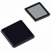
ADUC847BCPZ8-5 Analog Devices Inc, ADUC847BCPZ8-5 Datasheet - Page 22

ADUC847BCPZ8-5
Manufacturer Part Number
ADUC847BCPZ8-5
Description
IC,Data Acquisition CODEC,2-CHANNEL,LLCC,56PIN,PLASTIC
Manufacturer
Analog Devices Inc
Series
MicroConverter® ADuC8xxr
Datasheet
1.EVAL-ADUC845QSZ.pdf
(108 pages)
Specifications of ADUC847BCPZ8-5
Core Processor
8052
Core Size
8-Bit
Speed
12.58MHz
Connectivity
I²C, SPI, UART/USART
Peripherals
POR, PSM, PWM, Temp Sensor, WDT
Number Of I /o
34
Program Memory Size
8KB (8K x 8)
Program Memory Type
FLASH
Eeprom Size
4K x 8
Ram Size
2.25K x 8
Voltage - Supply (vcc/vdd)
4.75 V ~ 5.25 V
Data Converters
A/D 10x24b; D/A 1x12b, 2x16b
Oscillator Type
Internal
Operating Temperature
-40°C ~ 85°C
Package / Case
56-LFCSP
Lead Free Status / RoHS Status
Lead free / RoHS Compliant
For Use With
EVAL-ADUC847QSZ - KIT DEV QUICK START FOR ADUC847
Lead Free Status / RoHS Status
Lead free / RoHS Compliant
ADuC845/ADuC847/ADuC848
Mnemoni
SJMP rel
JC rel
JNC rel
JZ rel
JNZ rel
DJNZ Rn,rel
LJMP
LCALL
JB bit,rel
JNB bit,rel
JBC bit,rel
CJNE A,dir,rel
CJNE A,#data,rel
CJNE Rn,#data,rel
CJNE @Ri,#data,rel
DJNZ dir,rel
Miscellaneous
NOP
1
2
3
MEMORY ORGANIZATION
The ADuC845, ADuC847, and ADuC848 contain four memory
blocks:
•
•
•
•
Flash/EE Program Memory
The parts provide up to 62 kbytes of Flash/EE program memory
to run user code. All further references to Flash/EE program
memory assume the 62-kbyte option.
When EA
hardware reset, the parts default to code execution from their
internal 62 kbytes of Flash/EE program memory. The parts do
not support the rollover from internal code space to external
code space. No external code space is available on the parts.
Permanently embedded firmware allows code to be serially
downloaded to the 62 kbytes of internal code space via the
UART serial port while the device is in-circuit. No external
hardware is required.
During run time, 56 kbytes of the 62-kbyte program memory
can be reprogrammed. This means that the code space can be
upgraded in the field by using a user-defined protocol running
on the parts, or it can be used as a data memory. For details, see
the Nonvolatile Flash/EE Memory Overview section.
One cycle is one clock.
MOVX instructions are four cycles when they have 0 wait state. Cycles of MOVX instructio
LCALL instructions are three cycles when the LCALL instruction comes from an interrupt.
62 kbytes/3
memory
4 kbytes of on-chip Flash/EE data memory
256 bytes of general-purpose RAM
2 kbytes of internal XRAM
3
addr16
c
is pulled high externally during a power cycle or a
2 kbytes/8 kbytes of on-chip Flas
Descri
Short jump (relative address)
Jump on carry = 1
Jump on carry = 0
Jump on accumulator = 0
Jump on accumulator ! = 0
Decrement register, JNZ relative
Long jump unconditional
Long jump to subroutine
Jump on direct bit = 1
Jump on direct bit = 0
Jump on direct bit = 1 and clear
Compare A, direct JNE rela
Compare A, immediate JNE relative
Compare register, immediate JNE relative
Compare indirect, immediate JNE relative
Decrement direct byte, JNZ relative
No operation
h/EE program
ption
Rev. B | Page 22 of 108
tive
Flash/EE Data Memory
The user has 4 kbytes of Flash/EE data memory available that
can be accessed indirectly by using a group of registers mapped
into the sp
the Nonvola
General-Purp e
The general-purpos
memories, the upp
lower 128 bytes of RAM can be accessed through direct or
indirect addressing. The upper 128 bytes of RAM can be
accessed only through indirect addressing because it shares th
same address space as the SFR space, which must be accessed
through direct addressing.
The lower 128 bytes of internal data memory are mapped as
shown in Figure 8. The lowest 32 bytes are grouped into four
banks of eight registers addressed as R0 to R7. The next 16 bytes
(128 bits), locations 20H to 2FH above the register banks, form
a block of directly addressable bit locations at Bit Addresses
00H to 7FH. The stack can be located anywhere in the internal
memory address space, and the stack depth can be expanded up
to 2048 bytes.
Reset initializes the stack pointer to location 07H. Any call or
push pre-increments the SP before loading the stack. Therefore,
loading the stack starts from location 08H, which is also the
first register (R0) of Register Bank 1. Thus, if one is going to use
more than one register bank, the stack pointer should be
initialized to an area of RAM not used for data storage.
ns are 4 + n cycles when they have n wait states as programmed via EW
ecial function register (SFR) space. For details, see
tile Flash/EE Memory Overview section.
os RAM
er a
e R
nd th
AM i
e lower 128 bytes of RAM. The
s divided into two separate
Bytes
2
2
2
2
2
2
3
3
3
3
3
3
3
3
3
3
1
Cycles
3
3
3
3
3
3
4
4
4
4
4
4
4
4
4
4
1
AIT.
1
e


