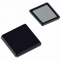
ADUC847BCPZ8-5 Analog Devices Inc, ADUC847BCPZ8-5 Datasheet - Page 95

ADUC847BCPZ8-5
Manufacturer Part Number
ADUC847BCPZ8-5
Description
IC,Data Acquisition CODEC,2-CHANNEL,LLCC,56PIN,PLASTIC
Manufacturer
Analog Devices Inc
Series
MicroConverter® ADuC8xxr
Datasheet
1.EVAL-ADUC845QSZ.pdf
(108 pages)
Specifications of ADUC847BCPZ8-5
Core Processor
8052
Core Size
8-Bit
Speed
12.58MHz
Connectivity
I²C, SPI, UART/USART
Peripherals
POR, PSM, PWM, Temp Sensor, WDT
Number Of I /o
34
Program Memory Size
8KB (8K x 8)
Program Memory Type
FLASH
Eeprom Size
4K x 8
Ram Size
2.25K x 8
Voltage - Supply (vcc/vdd)
4.75 V ~ 5.25 V
Data Converters
A/D 10x24b; D/A 1x12b, 2x16b
Oscillator Type
Internal
Operating Temperature
-40°C ~ 85°C
Package / Case
56-LFCSP
Lead Free Status / RoHS Status
Lead free / RoHS Compliant
For Use With
EVAL-ADUC847QSZ - KIT DEV QUICK START FOR ADUC847
Lead Free Status / RoHS Status
Lead free / RoHS Compliant
TIMING SPECIFICATIONS
AC inputs during testing are driven at DV
Logic 1 and V
For timing purposes, a port pin is no longer floating when a 100 mV change from load voltage occurs. A port pin begins to float when a
100 mV change from the loaded V
C
AV
noted.
Table 64. CLOCK INPUT (External Clock Driven XTAL1) Parameter
t
t
t
t
t
1/t
t
t
1
2
3
CK
CKL
CKH
CKR
CKF
CORE
CYC
ADuC845/ADuC847/ADuC848 internal PLL locks onto a multiple (512 times) of the 32.768 kHz external crystal frequency to provide a stable 12.58 MHz internal clock
for the system. The core can operate at this frequency or at a binary submultiple called Core_Clk, selected via the PLLCON SFR.
This number is measured at the default Core_Clk operating frequency of 1.57 MHz.
ADuC845/ADuC847/ADuC848 machine cycle time is nominally defined as 1/Core_Clk.
LOAD
CORE
DD
= 2.7 V to 3.6 V or 4.75 V to 5.25 V, DV
for all outputs = 80 pF, unless otherwise noted.
IL
max for Logic 0 as shown in Figure 72.
DV
DD
– 0.5V
0.45V
XTAL1 Period
XTAL1 Width Low
XTAL1 Width High
XTAL1 Rise Time
XTAL1 Fall Time
Core Clock Frequency
Core Clock Period
Machine Cycle Time
OH
/V
0.2DV
0.2DV
OL
TEST POINTS
level occurs as shown in Figure 72.
DD
2
DD
DD
– 0.5 V for Logic 1 and 0.45 V for Logic 0. Timing measurements are made at V
3
– 0.1V
DD
+ 0.9V
1
= 2.7 V to 3.6 V or 4.75 V to 5.25 V; all specifications T
Figure 72. Timing Waveform Characteristics
Rev. B | Page 95 of 108
V
LOAD
V
V
LOAD
LOAD
– 0.1V
+ 0.1V
Min
0.098
10.2
REFERENCE
POINTS
TIMING
32.768 kHz External Crystal
ADuC845/ADuC847/ADuC848
Typ
30.52
6.26
6.26
9
9
1.57
0.636
0.636
MIN
V
V
LOAD
LOAD
to T
– 0.1V
– 0.1V
MAX
V
Max
12.58
0.08
, unless otherwise
LOAD
IH
min for
Unit
µs
µs
µs
ns
ns
µs
µs
MHz


