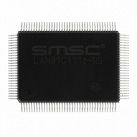
LAN91C111I-NS SMSC, LAN91C111I-NS Datasheet - Page 20

LAN91C111I-NS
Manufacturer Part Number
LAN91C111I-NS
Description
IC ETHERNET CTLR MAC PHY 128-QFP
Manufacturer
SMSC
Type
Single Chip MAC and PHYr
Datasheet
1.LAN91C111-NU.pdf
(128 pages)
Specifications of LAN91C111I-NS
Controller Type
Ethernet Controller, MAC/PHY
Interface
Serial EEPROM
Voltage - Supply
3.3V
Operating Temperature
-40°C ~ 85°C
Mounting Type
Surface Mount
Package / Case
128-QFP
Product
Ethernet Controllers
Number Of Transceivers
1
Standard Supported
IEEE 802.3 or IEEE 802.3u
Data Rate
10 Mbps or 100 Mbps
Supply Voltage (max)
5 V
Supply Voltage (min)
0 V
Supply Current (max)
140 mA
Maximum Operating Temperature
+ 85 C
Ethernet Connection Type
100BASE-T or 100BASE-T4 or 100BASE-TX or 10BASE-T
Minimum Operating Temperature
- 40 C
Mounting Style
SMD/SMT
Lead Free Status / RoHS Status
Lead free / RoHS Compliant
Current - Supply
-
Lead Free Status / Rohs Status
Lead free / RoHS Compliant
Other names
638-1014
Available stocks
Company
Part Number
Manufacturer
Quantity
Price
Company:
Part Number:
LAN91C111I-NS
Manufacturer:
RECOM
Quantity:
1 000
Company:
Part Number:
LAN91C111I-NS
Manufacturer:
SMSC
Quantity:
1 000
Company:
Part Number:
LAN91C111I-NS
Manufacturer:
Standard
Quantity:
6 916
Company:
Part Number:
LAN91C111I-NS
Manufacturer:
Microchip Technology
Quantity:
10 000
Chapter 7 Functional Description
Revision 1.91 (06-01-09)
7.1
7.2
7.2.1
7.2.2
7.3
Clock Generator Block
CSMA/CD Block
MMU Block
1. The XTAL1 and XTAL2 pins are to be connected to a 25 MHz crystal.
2. TX25 is an input clock. It will be the nibble rate of the particular PHY connected to the MII (2.5
3. RX25 - This is the MII nibble rate receive clock used for sampling received data nibbles and
4. LCLK - Bus clock - Used by the BIU for synchronous accesses. Maximum frequency is 50 MHz
This is a 16 bit oriented block, with fully- independent Transmit and Receive logic. The data path in
and out of the block consists of two 16-bit wide uni-directional FIFOs interfacing the DMA block. The
DMA port of the FIFO stores 32 bits to exploit the 32 bit data path into memory, but the FIFOs
themselves are 16 bit wide. The Control Path consists of a set of registers interfaced to the CPU via
the BIU.
DMA Block
This block accesses packet memory on the CSMA/CD’s behalf, fetching transmit data and storing
received data. It interfaces the CSMA/CD Transmit and Receive FIFOs on one side and the Arbiter
block on the other. To increase the bandwidth into memory, a 50 MHz clock is used by the DMA block,
and the data path is 32 bits wide.
For example, during active reception at 100 Mbps, the CSMA/CD block will write a word into the
Receive FIFO every 160ns. The DMA will read the FIFO and accumulate two words on the output port
to request a memory cycle from the Arbiter every 320ns.
The DMA machine is able to support full duplex operation. Independent receive and transmit counters
are used. Transmit and receive cycles are alternated when simultaneous receive and transmit
accesses are needed.
Arbiter Block
The Arbiter block sequences accesses to packet RAM requested by the BIU and by the DMA blocks.
BIU requests represent pipelined CPU accesses to the Data Register, while DMA requests represent
CSMA/CD data movement.
Internal SRAM read accesses are always 32 bit wide, and the Arbiter steers the appropriate byte(s) to
the appropriate lanes as a function of the address.
The CPU Data Path consists of two uni-directional FIFOs mapped at the Data Register location. These
FIFOs can be accessed in any combination of bytes, word, or doublewords. The Arbiter will indicate
'Not Ready' whenever a cycle is initiated that cannot be satisfied by the present state of the FIFO.
The Hardware Memory Management Unit allocates memory and transmit and receive packet queues.
It also determines the value of the transmit and receive interrupts as a function of the queues. The
page size is 2048 bytes, with a maximum memory size of 8kbytes. MIR values are interpreted in 2048
byte units.
MHz for a 10 Mbps PHY, and 25 MHz for a 100 Mbps PHY).
running the receive state machine. (2.5 MHz for a 10 Mbps PHY, and 25 MHz for a 100 Mbps PHY).
for VL BUS mode, and 8.33 MHz for EISA slave DMA.
DATASHEET
20
10/100 Non-PCI Ethernet Single Chip MAC + PHY
SMSC LAN91C111 REV C
Datasheet


