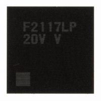
DF2117VLP20V Renesas Electronics America, DF2117VLP20V Datasheet - Page 16

DF2117VLP20V
Manufacturer Part Number
DF2117VLP20V
Description
IC H8S/2117 MCU FLASH 145TFLGA
Manufacturer
Renesas Electronics America
Series
H8® H8S/2100r
Datasheet
1.DF2117VBG20V.pdf
(960 pages)
Specifications of DF2117VLP20V
Core Processor
H8S/2600
Core Size
16-Bit
Speed
20MHz
Connectivity
FIFO, I²C, LPC, SCI, SmartCard
Peripherals
POR, PWM, WDT
Number Of I /o
112
Program Memory Size
160KB (160K x 8)
Program Memory Type
FLASH
Ram Size
8K x 8
Voltage - Supply (vcc/vdd)
3 V ~ 3.6 V
Data Converters
A/D 16x10b
Oscillator Type
External
Operating Temperature
-20°C ~ 75°C
Package / Case
145-TFLGA
For Use With
HS0005KCU11H - EMULATOR E10A-USB H8S(X),SH2(A)3DK2166 - DEV EVAL KIT H8S/2166
Lead Free Status / RoHS Status
Lead free / RoHS Compliant
Eeprom Size
-
Available stocks
Company
Part Number
Manufacturer
Quantity
Price
Company:
Part Number:
DF2117VLP20V
Manufacturer:
Renesas
Quantity:
100
Part Number:
DF2117VLP20V
Manufacturer:
RENESAS/瑞萨
Quantity:
20 000
- Current page: 16 of 960
- Download datasheet (6Mb)
Rev. 3.00 Sep. 28, 2009 Page xiv of xliv
REJ09B0350-0300
Item
15.6.5 Simultaneous Serial Data
Transmission and Reception
(Clocked Synchronous Mode)
Figure 15.20 Sample Flowchart
of Simultaneous Serial
Transmission and Reception
16.3.8 FIFO Control Register
(FFCR)
16.4.4 Data Transmission/
Reception with Flow Control
Figure 16.6 Example of
Initialization Flowchart
Figure 16.10 Example of Data
Reception Flowchart
16.6.2 FLCR Access During
Serial Transmission and
Reception
Page Revision (See Manual for Details)
447
476
493
497
502
Figure amended
Table amended
Figure amended
Figure amended
Newly added
Bit
2
1
(Transmission/reception standby flow)
Bit Name
XMITFRST
RCVRFRST
Receive data ready interrupt
[5] Select parity with the EPS and PEN bits in FLCR, and
[6] Set the FIFOE bit in FFCR to 1 to enable the FIFO.
Read receive FIFO
PE = 1, or OE = 1
BI = 1, FE = 1,
Read FLSR
Read FLSR
set the stop bit with the STOP bit in FLCR. Then, set
the data length with the CLS1 and CLS0 bits in FLCR.
Set the receive FIFO trigger level with the RCVRTRIG1
and RCVRTRIG0 bits in FFCR. Select the best trigger
level to prevent an overflow of the receive FIFO.
DR = 0
No
No
Initial Value
0
0
Clear TE and RE bits in SCR to 0
End transmission/reception
Yes
All data received?
R/W
R/W
R/W
Error processing
[1]
[2]
[3]
[4]
Description
Transmit FIFO Reset
The transmit FIFO data is cleared when 1 is written.
However, FTSR data is not cleared. This bit is
automatically cleared.
Receive FIFO Reset
The receive FIFO data is cleared when 1 is written.
However, FRSR data is not cleared.
This bit is automatically cleared.
Yes
[1] When data is received, a receive data ready
[2] Confirm that the BI, FE, PE, and OE flags in
[3] Read the receive FIFO.
[4] Check the DR flag in FLSR. When the DR flag
interrupt occurs. Go to the data reception flow
by using this interrupt trigger.
FLSR are all cleared. If any one of these flags
is set to 1, perform error processing.
is cleared and all of the data has been read, data
reception is complete.
[5]
[6]
Related parts for DF2117VLP20V
Image
Part Number
Description
Manufacturer
Datasheet
Request
R

Part Number:
Description:
KIT STARTER FOR M16C/29
Manufacturer:
Renesas Electronics America
Datasheet:

Part Number:
Description:
KIT STARTER FOR R8C/2D
Manufacturer:
Renesas Electronics America
Datasheet:

Part Number:
Description:
R0K33062P STARTER KIT
Manufacturer:
Renesas Electronics America
Datasheet:

Part Number:
Description:
KIT STARTER FOR R8C/23 E8A
Manufacturer:
Renesas Electronics America
Datasheet:

Part Number:
Description:
KIT STARTER FOR R8C/25
Manufacturer:
Renesas Electronics America
Datasheet:

Part Number:
Description:
KIT STARTER H8S2456 SHARPE DSPLY
Manufacturer:
Renesas Electronics America
Datasheet:

Part Number:
Description:
KIT STARTER FOR R8C38C
Manufacturer:
Renesas Electronics America
Datasheet:

Part Number:
Description:
KIT STARTER FOR R8C35C
Manufacturer:
Renesas Electronics America
Datasheet:

Part Number:
Description:
KIT STARTER FOR R8CL3AC+LCD APPS
Manufacturer:
Renesas Electronics America
Datasheet:

Part Number:
Description:
KIT STARTER FOR RX610
Manufacturer:
Renesas Electronics America
Datasheet:

Part Number:
Description:
KIT STARTER FOR R32C/118
Manufacturer:
Renesas Electronics America
Datasheet:

Part Number:
Description:
KIT DEV RSK-R8C/26-29
Manufacturer:
Renesas Electronics America
Datasheet:

Part Number:
Description:
KIT STARTER FOR SH7124
Manufacturer:
Renesas Electronics America
Datasheet:

Part Number:
Description:
KIT STARTER FOR H8SX/1622
Manufacturer:
Renesas Electronics America
Datasheet:

Part Number:
Description:
KIT DEV FOR SH7203
Manufacturer:
Renesas Electronics America
Datasheet:


