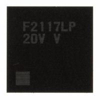
DF2117VLP20V Renesas Electronics America, DF2117VLP20V Datasheet - Page 922

DF2117VLP20V
Manufacturer Part Number
DF2117VLP20V
Description
IC H8S/2117 MCU FLASH 145TFLGA
Manufacturer
Renesas Electronics America
Series
H8® H8S/2100r
Datasheet
1.DF2117VBG20V.pdf
(960 pages)
Specifications of DF2117VLP20V
Core Processor
H8S/2600
Core Size
16-Bit
Speed
20MHz
Connectivity
FIFO, I²C, LPC, SCI, SmartCard
Peripherals
POR, PWM, WDT
Number Of I /o
112
Program Memory Size
160KB (160K x 8)
Program Memory Type
FLASH
Ram Size
8K x 8
Voltage - Supply (vcc/vdd)
3 V ~ 3.6 V
Data Converters
A/D 16x10b
Oscillator Type
External
Operating Temperature
-20°C ~ 75°C
Package / Case
145-TFLGA
For Use With
HS0005KCU11H - EMULATOR E10A-USB H8S(X),SH2(A)3DK2166 - DEV EVAL KIT H8S/2166
Lead Free Status / RoHS Status
Lead free / RoHS Compliant
Eeprom Size
-
Available stocks
Company
Part Number
Manufacturer
Quantity
Price
Company:
Part Number:
DF2117VLP20V
Manufacturer:
Renesas
Quantity:
100
Part Number:
DF2117VLP20V
Manufacturer:
RENESAS/瑞萨
Quantity:
20 000
- Current page: 922 of 960
- Download datasheet (6Mb)
Section 26 Electrical Characteristics
26.2
Table 26.2 lists the DC characteristics. Table 26.3 lists the permissible output currents. Table 26.4
lists the bus drive characteristics.
Table 26.2 DC Characteristics (1)
Conditions: V
Rev. 3.00 Sep. 28, 2009 Page 876 of 910
REJ09B0350-0300
Item
Schmitt trigger
input voltage
Input high voltage
Input low voltage
Output high
voltage
Output low
voltage
DC Characteristics
V
CC
SS
P67 to P60,
IRQ7 to IRQ0, IRQ15 to IRQ8
KIN7 to KIN0, KIN15 to KIN8,
WUE15 to WUE8
ExIRQ7 to ExIRQ6, and
ExIRQ15 to ExIRQ8
RES, NMI, MD2, MD1, and
ETRST
EXTAL
Port 7
Ports A, G, I, PE4, PE2 to
PE0, P97, P86, P52, and P42
Input pins other than (1) and
(2) above
RES, MD2, MD1, and ETRST (3)
NMI, EXTAL, and input pins other
than (1) and (3) above
All output pins (except for ports A,
G, I, P97, P86, P52, and P42)
Ports A, G, I, P97, P86, P52, and
P42*
All output pins *
Ports 1, 2, 3, C, and D
= AV
= 3.0 V to 3.6 V, AV
2
SS
*
1
= 0 V
3
CC
(1)
(2)
*
1
= 3.0 V to 3.6 V, AVref*
Symbol
V
V
V
V
V
V
V
T
T
T
I H
IL
OH
OL
–
+
+
– V
T
–
Min.
V
⎯
V
V
V
AV
V
V
– 0.3
–0.3
V
V
0.5
⎯
⎯
CC
CC
CC
CC
CC
CC
CC
CC
CC
× 0.2
× 0.05
× 0.9
× 0.7
× 0.7
× 0.7
– 0.5
– 1.0
× 0.7
Typ.
⎯
⎯
⎯
⎯
⎯
⎯
⎯
⎯
⎯
⎯
⎯
⎯
⎯
⎯
⎯
1
= 3.0 V to AV
Max.
⎯
V
⎯
V
V
AV
5.5
V
V
V
⎯
⎯
⎯
0.4
1.0
CC
CC
CC
CC
CC
CC
CC
× 0.7
+ 0.3
+ 0.3
+ 0.3
× 0.1
× 0.2
+ 0.3
Unit
V
CC
,
Test
Conditions
I
I
I
I
I
OH
OH
OH
OL
OL
= 1.6 mA
= 5 mA
= –200 μA
= –1 mA
= - 200 μA
Related parts for DF2117VLP20V
Image
Part Number
Description
Manufacturer
Datasheet
Request
R

Part Number:
Description:
KIT STARTER FOR M16C/29
Manufacturer:
Renesas Electronics America
Datasheet:

Part Number:
Description:
KIT STARTER FOR R8C/2D
Manufacturer:
Renesas Electronics America
Datasheet:

Part Number:
Description:
R0K33062P STARTER KIT
Manufacturer:
Renesas Electronics America
Datasheet:

Part Number:
Description:
KIT STARTER FOR R8C/23 E8A
Manufacturer:
Renesas Electronics America
Datasheet:

Part Number:
Description:
KIT STARTER FOR R8C/25
Manufacturer:
Renesas Electronics America
Datasheet:

Part Number:
Description:
KIT STARTER H8S2456 SHARPE DSPLY
Manufacturer:
Renesas Electronics America
Datasheet:

Part Number:
Description:
KIT STARTER FOR R8C38C
Manufacturer:
Renesas Electronics America
Datasheet:

Part Number:
Description:
KIT STARTER FOR R8C35C
Manufacturer:
Renesas Electronics America
Datasheet:

Part Number:
Description:
KIT STARTER FOR R8CL3AC+LCD APPS
Manufacturer:
Renesas Electronics America
Datasheet:

Part Number:
Description:
KIT STARTER FOR RX610
Manufacturer:
Renesas Electronics America
Datasheet:

Part Number:
Description:
KIT STARTER FOR R32C/118
Manufacturer:
Renesas Electronics America
Datasheet:

Part Number:
Description:
KIT DEV RSK-R8C/26-29
Manufacturer:
Renesas Electronics America
Datasheet:

Part Number:
Description:
KIT STARTER FOR SH7124
Manufacturer:
Renesas Electronics America
Datasheet:

Part Number:
Description:
KIT STARTER FOR H8SX/1622
Manufacturer:
Renesas Electronics America
Datasheet:

Part Number:
Description:
KIT DEV FOR SH7203
Manufacturer:
Renesas Electronics America
Datasheet:


