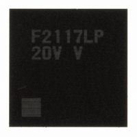
DF2117VLP20V Renesas Electronics America, DF2117VLP20V Datasheet - Page 621

DF2117VLP20V
Manufacturer Part Number
DF2117VLP20V
Description
IC H8S/2117 MCU FLASH 145TFLGA
Manufacturer
Renesas Electronics America
Series
H8® H8S/2100r
Datasheet
1.DF2117VBG20V.pdf
(960 pages)
Specifications of DF2117VLP20V
Core Processor
H8S/2600
Core Size
16-Bit
Speed
20MHz
Connectivity
FIFO, I²C, LPC, SCI, SmartCard
Peripherals
POR, PWM, WDT
Number Of I /o
112
Program Memory Size
160KB (160K x 8)
Program Memory Type
FLASH
Ram Size
8K x 8
Voltage - Supply (vcc/vdd)
3 V ~ 3.6 V
Data Converters
A/D 16x10b
Oscillator Type
External
Operating Temperature
-20°C ~ 75°C
Package / Case
145-TFLGA
For Use With
HS0005KCU11H - EMULATOR E10A-USB H8S(X),SH2(A)3DK2166 - DEV EVAL KIT H8S/2166
Lead Free Status / RoHS Status
Lead free / RoHS Compliant
Eeprom Size
-
Available stocks
Company
Part Number
Manufacturer
Quantity
Price
Company:
Part Number:
DF2117VLP20V
Manufacturer:
Renesas
Quantity:
100
Part Number:
DF2117VLP20V
Manufacturer:
RENESAS/瑞萨
Quantity:
20 000
- Current page: 621 of 960
- Download datasheet (6Mb)
18.4.2
In a transmit operation, KCLK (clock) is an output on the keyboard side, and KD (data) is an
output on the chip (system) side. KD outputs a start bit, 8 data bits (LSB-first), an odd parity bit,
and a stop bit, in that order. The KD value is valid when KCLK is high. A sample transmit
processing flowchart is shown in figure 18.5, and the transmit timing in figure 18.6.
Autmatic transmission
(reception disabled)
Write transmit data
Both KCLKI and
Clear I/O inhibit
Clear KBTE bit
Set KBIOE bit
Read KBCRH
Clear KBE bit
Set I/O inhibit
Read KBCRH
(KCLKO = 0)
(KCLKO = 1)
Set start bit
(KDO = 0)*
To transmit operation or receive operation
(KBTS = 1)
Transmit Operation
KBTE = 1
KTER = 0
Set KBTS
KDI = 1?
KDI = 1?
to KBTR
Start
Yes
Yes
Yes
Yes
Figure 18.5 Sample Transmit Processing Flowchart
No
No
No
[11]
[10]
KDO retains 1
No
KCLKO retains 0
KDO retains 0
(Condition: KBE = 0)
[1]
[2]
[3]
[4]
[5]
[6]
[7]
[8]
processing execution
processing execution
[9]
Receive termination
Retransmit request
Error handling
Note: * The start bit (KDO = 0) is automatically initialized (KDO = 1)
[1]
[2]
[3]
[4]
[5]
[6]
[7]
[8]
[9]
[10]
[11]
when automatic transmission is started. After initialization,
to write 0 to KDO, read 1 before writing 0 to it.
Write 1 to the KBIOE bit to enable transmission/
reception.
Clear the KBE bit (reception disabled).
Write transmit data to KBTR.
Read KBCRH, and when both the KCLKI and
KDI bits are 1, write 0 to the KCLKO bit to set
the I/O inhibit. 60 μs or more is required for I/O
inhibit.
Read KBCRH, and when the KDI bit is 1, write
0 to the KDO (set start bit).
Write 1 to the KBTS bit to enter the transmit
enabled state.
Write 1 to the KCLKO bit to clear the I/O inhibit.
Check D0 to D7, the parity bit, the stop bit, and
receive completion notification (send data at the
falling edge of the KCLK signal).
The KBTE bit is set to 1 at the eleventh rising
edge of the KCLK signal. When KTIE = 1, a
CPU interrupt occurs.
When KTER = 0, transmission is successfully completed.
Clear the KBTE bit to 0.
Section 18 Keyboard Buffer Control Unit (PS2)
Rev. 3.00 Sep. 28, 2009 Page 575 of 910
REJ09B0350-0300
Related parts for DF2117VLP20V
Image
Part Number
Description
Manufacturer
Datasheet
Request
R

Part Number:
Description:
KIT STARTER FOR M16C/29
Manufacturer:
Renesas Electronics America
Datasheet:

Part Number:
Description:
KIT STARTER FOR R8C/2D
Manufacturer:
Renesas Electronics America
Datasheet:

Part Number:
Description:
R0K33062P STARTER KIT
Manufacturer:
Renesas Electronics America
Datasheet:

Part Number:
Description:
KIT STARTER FOR R8C/23 E8A
Manufacturer:
Renesas Electronics America
Datasheet:

Part Number:
Description:
KIT STARTER FOR R8C/25
Manufacturer:
Renesas Electronics America
Datasheet:

Part Number:
Description:
KIT STARTER H8S2456 SHARPE DSPLY
Manufacturer:
Renesas Electronics America
Datasheet:

Part Number:
Description:
KIT STARTER FOR R8C38C
Manufacturer:
Renesas Electronics America
Datasheet:

Part Number:
Description:
KIT STARTER FOR R8C35C
Manufacturer:
Renesas Electronics America
Datasheet:

Part Number:
Description:
KIT STARTER FOR R8CL3AC+LCD APPS
Manufacturer:
Renesas Electronics America
Datasheet:

Part Number:
Description:
KIT STARTER FOR RX610
Manufacturer:
Renesas Electronics America
Datasheet:

Part Number:
Description:
KIT STARTER FOR R32C/118
Manufacturer:
Renesas Electronics America
Datasheet:

Part Number:
Description:
KIT DEV RSK-R8C/26-29
Manufacturer:
Renesas Electronics America
Datasheet:

Part Number:
Description:
KIT STARTER FOR SH7124
Manufacturer:
Renesas Electronics America
Datasheet:

Part Number:
Description:
KIT STARTER FOR H8SX/1622
Manufacturer:
Renesas Electronics America
Datasheet:

Part Number:
Description:
KIT DEV FOR SH7203
Manufacturer:
Renesas Electronics America
Datasheet:


