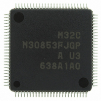
M30853FJGP#U3 Renesas Electronics America, M30853FJGP#U3 Datasheet - Page 189

M30853FJGP#U3
Manufacturer Part Number
M30853FJGP#U3
Description
IC M32C MCU FLASH 100LQFP
Manufacturer
Renesas Electronics America
Series
M16C™ M32C/80r
Datasheets
1.M3087BFLGPU3.pdf
(364 pages)
2.M30853FHFPD5.pdf
(94 pages)
3.M30853FHFPU3.pdf
(544 pages)
Specifications of M30853FJGP#U3
Core Processor
M32C/80
Core Size
16/32-Bit
Speed
32MHz
Connectivity
CAN, I²C, IEBus, SIO, UART/USART
Peripherals
DMA, WDT
Number Of I /o
85
Program Memory Size
512KB (512K x 8)
Program Memory Type
FLASH
Ram Size
24K x 8
Voltage - Supply (vcc/vdd)
3 V ~ 5.5 V
Data Converters
A/D 26x10b; D/A 2x8b
Oscillator Type
Internal
Operating Temperature
-40°C ~ 85°C
Package / Case
100-LQFP
For Use With
R0K330879S001BE - KIT DEV RSK M32C/87R0K330879S000BE - KIT DEV RSK M32C/87
Lead Free Status / RoHS Status
Lead free / RoHS Compliant
Eeprom Size
-
Available stocks
Company
Part Number
Manufacturer
Quantity
Price
Part Number:
M30853FJGP#U3M30853FJGP#D5
Manufacturer:
Renesas Electronics America
Quantity:
10 000
- Current page: 189 of 544
- Download datasheet (4Mb)
R
R
M
e
E
3
. v
J
2
Figure 15.9 TA0MR to TA4MR Registers
0
C
1
9
0 .
8 /
B
0
3
5
0
3
G
J
7
u
o r
0 -
. l
Timer Ai Mode Register
b7
NOTES:
u
0
1
p
, 1
0
b6
1. The TAiTGH and TAiTGL bits in the ONSF or TRGSR register determine the count source in the event
2. MR1 bit setting is enabled only when counting how many times external signals are applied.
3. The timer decrements a counter value when an "L" signal is applied to the TA
4. The TCK1 bit is enabled only in the TA3MR register.
5. For two-phase pulse signal processing, set the TAjP bit in the UDF register (j=2 to 4) to "1" (two-phase
3
(
2
M
counter mode.
increments a counter value when an "H" signal is applied to the TA
pulse signal processing function enabled). Also, set the TAiTGH and TAiTGL bits to "00
TAj
b5
0
0
3
0
IN
5
2
b4
C
pin).
8 /
b3
Page 164
, 5
b2
0
M
3
b1
0
2
C
b0
1
f o
8 /
4
5
TMOD0
TMOD1
Symbol
9
TCK0
TCK1
) T
MR1
MR2
MR3
(b2)
4
Bit
Symbol
TA0MR to TA4MR
(i=0 to 4)
Operating Mode
Select Bit
Reserved Bit
Count Polarity
Select Bit
Increment/Decrement
Switching Source
Select Bit
Two-Phase Pulse
Signal Processing
Operation Select Bit
Count Operation
Type Select Bit
Set to "0" in event counter mode
Bit Name
(Event Counter Mode)
(2)
Address
0356
(4,5)
16
, 0357
b1b0
Set to "0"
0 : Counts falling edges
1 : Counts rising edges
0 : UDF registser
1 : Input signal to
0 : Reloading
1 : Free running
0 1 : Event counter mode
Set to "0"
two-phase pulse signal)
(When not processing
of an external signal
of an external signal
setting
TAi
16
, 0358
Function
OUT
pin
16
, 0359
iOUT
(3)
pin.
16
, 035A
0 : Normal processing
1 : Multiply-by-4
Set to "0"
Set to "1"
two-phase pulse signal)
iOUT
(When processing
operation
processing operation
(1)
16
Function
pin and the timer
After Reset
00
16
2
" (input to the
15. Timer (Timer A)
RW
RW
RW
RW
RW
RW
RW
RW
RW
Related parts for M30853FJGP#U3
Image
Part Number
Description
Manufacturer
Datasheet
Request
R

Part Number:
Description:
KIT STARTER FOR M16C/29
Manufacturer:
Renesas Electronics America
Datasheet:

Part Number:
Description:
KIT STARTER FOR R8C/2D
Manufacturer:
Renesas Electronics America
Datasheet:

Part Number:
Description:
R0K33062P STARTER KIT
Manufacturer:
Renesas Electronics America
Datasheet:

Part Number:
Description:
KIT STARTER FOR R8C/23 E8A
Manufacturer:
Renesas Electronics America
Datasheet:

Part Number:
Description:
KIT STARTER FOR R8C/25
Manufacturer:
Renesas Electronics America
Datasheet:

Part Number:
Description:
KIT STARTER H8S2456 SHARPE DSPLY
Manufacturer:
Renesas Electronics America
Datasheet:

Part Number:
Description:
KIT STARTER FOR R8C38C
Manufacturer:
Renesas Electronics America
Datasheet:

Part Number:
Description:
KIT STARTER FOR R8C35C
Manufacturer:
Renesas Electronics America
Datasheet:

Part Number:
Description:
KIT STARTER FOR R8CL3AC+LCD APPS
Manufacturer:
Renesas Electronics America
Datasheet:

Part Number:
Description:
KIT STARTER FOR RX610
Manufacturer:
Renesas Electronics America
Datasheet:

Part Number:
Description:
KIT STARTER FOR R32C/118
Manufacturer:
Renesas Electronics America
Datasheet:

Part Number:
Description:
KIT DEV RSK-R8C/26-29
Manufacturer:
Renesas Electronics America
Datasheet:

Part Number:
Description:
KIT STARTER FOR SH7124
Manufacturer:
Renesas Electronics America
Datasheet:

Part Number:
Description:
KIT STARTER FOR H8SX/1622
Manufacturer:
Renesas Electronics America
Datasheet:

Part Number:
Description:
KIT DEV FOR SH7203
Manufacturer:
Renesas Electronics America
Datasheet:


