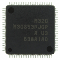
M30853FJGP#U3 Renesas Electronics America, M30853FJGP#U3 Datasheet - Page 224

M30853FJGP#U3
Manufacturer Part Number
M30853FJGP#U3
Description
IC M32C MCU FLASH 100LQFP
Manufacturer
Renesas Electronics America
Series
M16C™ M32C/80r
Datasheets
1.M3087BFLGPU3.pdf
(364 pages)
2.M30853FHFPD5.pdf
(94 pages)
3.M30853FHFPU3.pdf
(544 pages)
Specifications of M30853FJGP#U3
Core Processor
M32C/80
Core Size
16/32-Bit
Speed
32MHz
Connectivity
CAN, I²C, IEBus, SIO, UART/USART
Peripherals
DMA, WDT
Number Of I /o
85
Program Memory Size
512KB (512K x 8)
Program Memory Type
FLASH
Ram Size
24K x 8
Voltage - Supply (vcc/vdd)
3 V ~ 5.5 V
Data Converters
A/D 26x10b; D/A 2x8b
Oscillator Type
Internal
Operating Temperature
-40°C ~ 85°C
Package / Case
100-LQFP
For Use With
R0K330879S001BE - KIT DEV RSK M32C/87R0K330879S000BE - KIT DEV RSK M32C/87
Lead Free Status / RoHS Status
Lead free / RoHS Compliant
Eeprom Size
-
Available stocks
Company
Part Number
Manufacturer
Quantity
Price
Part Number:
M30853FJGP#U3M30853FJGP#D5
Manufacturer:
Renesas Electronics America
Quantity:
10 000
- Current page: 224 of 544
- Download datasheet (4Mb)
M
R
R
e
E
3
. v
J
2
Figure 17.8 U0SMR4 to U4SMR4 Registers
0
C
1
9
0 .
8 /
B
0
3
5
0
3
G
J
7
u
o r
0 -
. l
UARTi Special Mode Register 4
b7
u
NOTES:
0
1
p
, 1
0
b6
3
1. When each condition is generated, the STAREQ, RSTAREQ or STPREQ bit is set to "0".
(
2
M
When a condition generation is incomplete, the bit remains unchanged as "1".
0
b5
3
0
5
2
b4
C
8 /
b3
Page 199
, 5
b2
M
3
b1
2
C
b0
f o
8 /
4
RSTAREQ
STPREQ
5
STAREQ
STSPSEL
9
Symbol
SCLHI
SWC9
) T
ACKD
ACKC
4
Bit
Symbol
U0SMR4 to U4SMR4
Start Condition
Generate Bit
Restart Condition
Generate Bit
Stop Condition
Generate Bit
SCL, SDA Output
Select Bit
ACK Data Bit
ACK Data Output
Enable Bit
SCL Output Stop
Enable Bit
SCL Wait Output Bit 3
Bit Name
(i=0 to 4)
(1)
(1)
(1)
Address
0364
16,
02E4
0: Clear
1: Start
0: Clear
1: Start
0: Clear
1: Start
0: Selects the serial I/O circuit
1: Selects the start/stop condition
0: ACK
1: NACK
0: Serial I/O data output
1: ACK data output
0: Disabled
1: Enabled
0: SCL "L" hold disabled
1: SCL "L" hold enabled
16,
generating circuit
0334
16,
0324
Function
16,
02F4
16
After Reset
00
16
RW
RW
RW
RW
RW
RW
RW
RW
RW
17. Serial I/O
Related parts for M30853FJGP#U3
Image
Part Number
Description
Manufacturer
Datasheet
Request
R

Part Number:
Description:
KIT STARTER FOR M16C/29
Manufacturer:
Renesas Electronics America
Datasheet:

Part Number:
Description:
KIT STARTER FOR R8C/2D
Manufacturer:
Renesas Electronics America
Datasheet:

Part Number:
Description:
R0K33062P STARTER KIT
Manufacturer:
Renesas Electronics America
Datasheet:

Part Number:
Description:
KIT STARTER FOR R8C/23 E8A
Manufacturer:
Renesas Electronics America
Datasheet:

Part Number:
Description:
KIT STARTER FOR R8C/25
Manufacturer:
Renesas Electronics America
Datasheet:

Part Number:
Description:
KIT STARTER H8S2456 SHARPE DSPLY
Manufacturer:
Renesas Electronics America
Datasheet:

Part Number:
Description:
KIT STARTER FOR R8C38C
Manufacturer:
Renesas Electronics America
Datasheet:

Part Number:
Description:
KIT STARTER FOR R8C35C
Manufacturer:
Renesas Electronics America
Datasheet:

Part Number:
Description:
KIT STARTER FOR R8CL3AC+LCD APPS
Manufacturer:
Renesas Electronics America
Datasheet:

Part Number:
Description:
KIT STARTER FOR RX610
Manufacturer:
Renesas Electronics America
Datasheet:

Part Number:
Description:
KIT STARTER FOR R32C/118
Manufacturer:
Renesas Electronics America
Datasheet:

Part Number:
Description:
KIT DEV RSK-R8C/26-29
Manufacturer:
Renesas Electronics America
Datasheet:

Part Number:
Description:
KIT STARTER FOR SH7124
Manufacturer:
Renesas Electronics America
Datasheet:

Part Number:
Description:
KIT STARTER FOR H8SX/1622
Manufacturer:
Renesas Electronics America
Datasheet:

Part Number:
Description:
KIT DEV FOR SH7203
Manufacturer:
Renesas Electronics America
Datasheet:


