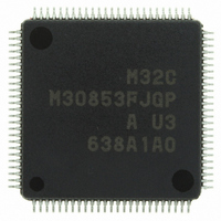
M30853FJGP#U3 Renesas Electronics America, M30853FJGP#U3 Datasheet - Page 525

M30853FJGP#U3
Manufacturer Part Number
M30853FJGP#U3
Description
IC M32C MCU FLASH 100LQFP
Manufacturer
Renesas Electronics America
Series
M16C™ M32C/80r
Datasheets
1.M3087BFLGPU3.pdf
(364 pages)
2.M30853FHFPD5.pdf
(94 pages)
3.M30853FHFPU3.pdf
(544 pages)
Specifications of M30853FJGP#U3
Core Processor
M32C/80
Core Size
16/32-Bit
Speed
32MHz
Connectivity
CAN, I²C, IEBus, SIO, UART/USART
Peripherals
DMA, WDT
Number Of I /o
85
Program Memory Size
512KB (512K x 8)
Program Memory Type
FLASH
Ram Size
24K x 8
Voltage - Supply (vcc/vdd)
3 V ~ 5.5 V
Data Converters
A/D 26x10b; D/A 2x8b
Oscillator Type
Internal
Operating Temperature
-40°C ~ 85°C
Package / Case
100-LQFP
For Use With
R0K330879S001BE - KIT DEV RSK M32C/87R0K330879S000BE - KIT DEV RSK M32C/87
Lead Free Status / RoHS Status
Lead free / RoHS Compliant
Eeprom Size
-
Available stocks
Company
Part Number
Manufacturer
Quantity
Price
Part Number:
M30853FJGP#U3M30853FJGP#D5
Manufacturer:
Renesas Electronics America
Quantity:
10 000
- Current page: 525 of 544
- Download datasheet (4Mb)
Rev.
REVISION HISTORY
Date
Page
284
285
287
288
289
291
293
294
295
297
298
299
300
303
308
315
335
336
344
345
358
359
• 21.3.1 Single-Phase Waveform Output Mode modified
• Figure 21.16 Single-Phase Waveform Output Mode modified
• Figure 21.17 Phase-Delayed Waveform Output Mode modified
• 21.3.3 Set/Reset Waveform Output modified
• Figure 21.18 SR Waveform Output Mode modified
• Figure 21.20 G0CR to G1CR Registers TXEPT bit in the G0CR register and b3
• Figure 21.22 G0MR to G1MR Registers b4 bit in the G1MR register changed
• Figure 21.23 G0EMR to G1EMR Registers Note 1 added to the G0EMR register;
• Figure 21.24 G0ETC to G1ETC Registers b0 to b2 in the G1ETC register
• Figure 21.26 G0IRF Register Note 1 and 2 added; b0 to b1, and b3 changed to
• Figure 21.27 G1IRF Register and G0TB to G1TB Registers b0 to b1 bits in
• Figure 21.28 G0CMP0 to GOCMP3, G1CMP0 to G1CMP3, G0MSK0 to
• Figure 21.29 CCS Register f1 added to clock selection: b4 to b7 bits changed
• Table 21.17 Pin Settings (2) PD8 register setting changed from PD8_2=0 to
• Table 21.25 HDLC Processing Mode Specifications CRC modified
CAN Module
• 22.1.1.3 BASICCAN Bit modified
• Figure 22.20 C0SSCTLR Register and C1SSCTLR Register Note 2 added
• Figure 22.21 C0SSSTR Register and C1SSSTR Register Note 1 added
• 22.1.20.4 REMACITVE Bit modified
• 22.1.20.5 RSPLOCK Bit modified
Programmable I/O Port
• 23.3 Function Select Register Aj (PSj Register, j= 0 to 5, 8, 9) modified
• 23.4 Function Select Register B0 to B3 (PSL0 toPSL3 Registers) modified
• 23.5 Function Select Register C (PSC, PSC2, PSC3 Registers) modified
• 23.6 Function Select Register D (PSD1 Register) modified
• 23.8 Port Control Register (PCR Register) modified
modified
to the PRY bit; b5 bit in the G1MR register changed to the PRYE bit
Note 2 modified
changed to RO bits; b3 changed to a RW bit; Note 1 added
RW bits
the G1IRF register changed to reserved bits; Note 2 modified; G1TB register
changed to G1DR register
GOMSK1, G1MSK0 to G1MSK1, G0TCRC to G1TCRC, G0RCRC to G1RCRC
Registers Note 1 modified and Note 2 added to the G0TCRC to G1TCRC register;
Note 1 and 3 in the G0RCRC to G1RCRC register modified
from reserved bits to bits with nothing assigned
PD8_0=0
M32C/85 Group(M32C/85, M32C/85T) Hardware Manual
C-6
Description
Summary
Related parts for M30853FJGP#U3
Image
Part Number
Description
Manufacturer
Datasheet
Request
R

Part Number:
Description:
KIT STARTER FOR M16C/29
Manufacturer:
Renesas Electronics America
Datasheet:

Part Number:
Description:
KIT STARTER FOR R8C/2D
Manufacturer:
Renesas Electronics America
Datasheet:

Part Number:
Description:
R0K33062P STARTER KIT
Manufacturer:
Renesas Electronics America
Datasheet:

Part Number:
Description:
KIT STARTER FOR R8C/23 E8A
Manufacturer:
Renesas Electronics America
Datasheet:

Part Number:
Description:
KIT STARTER FOR R8C/25
Manufacturer:
Renesas Electronics America
Datasheet:

Part Number:
Description:
KIT STARTER H8S2456 SHARPE DSPLY
Manufacturer:
Renesas Electronics America
Datasheet:

Part Number:
Description:
KIT STARTER FOR R8C38C
Manufacturer:
Renesas Electronics America
Datasheet:

Part Number:
Description:
KIT STARTER FOR R8C35C
Manufacturer:
Renesas Electronics America
Datasheet:

Part Number:
Description:
KIT STARTER FOR R8CL3AC+LCD APPS
Manufacturer:
Renesas Electronics America
Datasheet:

Part Number:
Description:
KIT STARTER FOR RX610
Manufacturer:
Renesas Electronics America
Datasheet:

Part Number:
Description:
KIT STARTER FOR R32C/118
Manufacturer:
Renesas Electronics America
Datasheet:

Part Number:
Description:
KIT DEV RSK-R8C/26-29
Manufacturer:
Renesas Electronics America
Datasheet:

Part Number:
Description:
KIT STARTER FOR SH7124
Manufacturer:
Renesas Electronics America
Datasheet:

Part Number:
Description:
KIT STARTER FOR H8SX/1622
Manufacturer:
Renesas Electronics America
Datasheet:

Part Number:
Description:
KIT DEV FOR SH7203
Manufacturer:
Renesas Electronics America
Datasheet:


