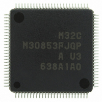
M30853FJGP#U3 Renesas Electronics America, M30853FJGP#U3 Datasheet - Page 538

M30853FJGP#U3
Manufacturer Part Number
M30853FJGP#U3
Description
IC M32C MCU FLASH 100LQFP
Manufacturer
Renesas Electronics America
Series
M16C™ M32C/80r
Datasheets
1.M3087BFLGPU3.pdf
(364 pages)
2.M30853FHFPD5.pdf
(94 pages)
3.M30853FHFPU3.pdf
(544 pages)
Specifications of M30853FJGP#U3
Core Processor
M32C/80
Core Size
16/32-Bit
Speed
32MHz
Connectivity
CAN, I²C, IEBus, SIO, UART/USART
Peripherals
DMA, WDT
Number Of I /o
85
Program Memory Size
512KB (512K x 8)
Program Memory Type
FLASH
Ram Size
24K x 8
Voltage - Supply (vcc/vdd)
3 V ~ 5.5 V
Data Converters
A/D 26x10b; D/A 2x8b
Oscillator Type
Internal
Operating Temperature
-40°C ~ 85°C
Package / Case
100-LQFP
For Use With
R0K330879S001BE - KIT DEV RSK M32C/87R0K330879S000BE - KIT DEV RSK M32C/87
Lead Free Status / RoHS Status
Lead free / RoHS Compliant
Eeprom Size
-
Available stocks
Company
Part Number
Manufacturer
Quantity
Price
Part Number:
M30853FJGP#U3M30853FJGP#D5
Manufacturer:
Renesas Electronics America
Quantity:
10 000
- Current page: 538 of 544
- Download datasheet (4Mb)
Rev.
REVISION HISTORY
Date
252-258
99-100
96-98
Page
113
115
116
123
113
137
145
156
188
192
210
211
241
246
248
246
246
289
314
85
87
Clock Generation Circuit
• Figure 9.6 TCSPR Register Value after reset revised
• Figure 9.8 PM2 Register Note 3 modified
• 9.5.2 Wait Mode Section structure modified; description modified
• 9.5.3 Stop Mode Section structure modified; description modified
Interrupts
• Figure 11.3 Interrupt Control Register(1) Some symbols modified
• Figure 11.5 RLVL Register Note 3 modified; value after reset revised
• 11.6.4 Interrupt Response Time The number of cycles in the description
• Figure 11.11 Key Input Interrupt Diagram modified
DMAC
• 13. DMAC Last sentence on the page modified
• Figure 13.3 DMD1 Register Value after reset modified
DMAC II
• Figure 14.1 RLVL Register Note 3 modified; value after reset revised
Timer (Timer A)
• Figure 15.5 TA0MR to TA4MR Register Value after reset revised
Three-Phase Motor Control Timer Function
• Figure 16.7 TB2MR Register Symbol revised
• Figure 16.8 Triangular Wave Modulation Operation Diagram modified
Serial I/O
• Figure 14.1 UARTi Block Diagram Diagram modified
• Figure 17.14 Transmit Operation Diagram modified
• Figure 17.15 Receive Operation Bit symbol in note 1 revised
• Figure 17.29 SIM Interface Operation Diagram modified
A/D Converter
• Figure 18.1 A/D Converter Block Diagram Diagram modified
• Figure 18.3 TA0MR to TA4MR Register Note 2 modified
• Tables 18.2 to 18.8 Mode Specification Note 1 deleted on all tables
D/A Converter
• Tables 19.3 D/A Converter Equivalent Circuit Diagram modified; the
Intelligent I/O
• Figure 22.4 G1BCR1 Register Value after reset revised
• Figure 22.15 Prescaler Function and Gate Function Diagram modified
• Figure 22.31 Transmit Operation Diagram modified
• Figure 22.32 Receive Operation Diagram modified
modifieddditional instructions added to the description
AD1CON1 register in note 4 deleted
M32C/85 Group(M32C/85, M32C/85T) Hardware Manual
C-19
Description
Summary
Related parts for M30853FJGP#U3
Image
Part Number
Description
Manufacturer
Datasheet
Request
R

Part Number:
Description:
KIT STARTER FOR M16C/29
Manufacturer:
Renesas Electronics America
Datasheet:

Part Number:
Description:
KIT STARTER FOR R8C/2D
Manufacturer:
Renesas Electronics America
Datasheet:

Part Number:
Description:
R0K33062P STARTER KIT
Manufacturer:
Renesas Electronics America
Datasheet:

Part Number:
Description:
KIT STARTER FOR R8C/23 E8A
Manufacturer:
Renesas Electronics America
Datasheet:

Part Number:
Description:
KIT STARTER FOR R8C/25
Manufacturer:
Renesas Electronics America
Datasheet:

Part Number:
Description:
KIT STARTER H8S2456 SHARPE DSPLY
Manufacturer:
Renesas Electronics America
Datasheet:

Part Number:
Description:
KIT STARTER FOR R8C38C
Manufacturer:
Renesas Electronics America
Datasheet:

Part Number:
Description:
KIT STARTER FOR R8C35C
Manufacturer:
Renesas Electronics America
Datasheet:

Part Number:
Description:
KIT STARTER FOR R8CL3AC+LCD APPS
Manufacturer:
Renesas Electronics America
Datasheet:

Part Number:
Description:
KIT STARTER FOR RX610
Manufacturer:
Renesas Electronics America
Datasheet:

Part Number:
Description:
KIT STARTER FOR R32C/118
Manufacturer:
Renesas Electronics America
Datasheet:

Part Number:
Description:
KIT DEV RSK-R8C/26-29
Manufacturer:
Renesas Electronics America
Datasheet:

Part Number:
Description:
KIT STARTER FOR SH7124
Manufacturer:
Renesas Electronics America
Datasheet:

Part Number:
Description:
KIT STARTER FOR H8SX/1622
Manufacturer:
Renesas Electronics America
Datasheet:

Part Number:
Description:
KIT DEV FOR SH7203
Manufacturer:
Renesas Electronics America
Datasheet:


