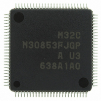
M30853FJGP#U3 Renesas Electronics America, M30853FJGP#U3 Datasheet - Page 386

M30853FJGP#U3
Manufacturer Part Number
M30853FJGP#U3
Description
IC M32C MCU FLASH 100LQFP
Manufacturer
Renesas Electronics America
Series
M16C™ M32C/80r
Datasheets
1.M3087BFLGPU3.pdf
(364 pages)
2.M30853FHFPD5.pdf
(94 pages)
3.M30853FHFPU3.pdf
(544 pages)
Specifications of M30853FJGP#U3
Core Processor
M32C/80
Core Size
16/32-Bit
Speed
32MHz
Connectivity
CAN, I²C, IEBus, SIO, UART/USART
Peripherals
DMA, WDT
Number Of I /o
85
Program Memory Size
512KB (512K x 8)
Program Memory Type
FLASH
Ram Size
24K x 8
Voltage - Supply (vcc/vdd)
3 V ~ 5.5 V
Data Converters
A/D 26x10b; D/A 2x8b
Oscillator Type
Internal
Operating Temperature
-40°C ~ 85°C
Package / Case
100-LQFP
For Use With
R0K330879S001BE - KIT DEV RSK M32C/87R0K330879S000BE - KIT DEV RSK M32C/87
Lead Free Status / RoHS Status
Lead free / RoHS Compliant
Eeprom Size
-
Available stocks
Company
Part Number
Manufacturer
Quantity
Price
Part Number:
M30853FJGP#U3M30853FJGP#D5
Manufacturer:
Renesas Electronics America
Quantity:
10 000
- Current page: 386 of 544
- Download datasheet (4Mb)
M
R
R
e
E
3
. v
J
2
Figure 23.34 C0SLOT0_6 to C0SLOT0_13, C0SLOT1_6 to C0SLOT1_13, C0SLOT0_14,
0
C
1
9
8 /
0 .
B
The message slot, selected by setting the CiSBS register, is read by reading the message slot buffer. A
message can be written in the message slot selected by the CiSBS register if the message is written to
the message slot buffer.
Write to the message slot k (k=0 to 15) while the corresponding CiMCTLk register is set to "00
0
3
5
0
G
3
J
7
u
CANi Message Slot Buffer j Data m
o r
CANi Message Slot Buffer j Time Stamp High-Ordered
CANi Message Slot Buffer j Time Stamp Low-Ordered
b7
0 -
. l
b7
b7
u
NOTES:
0
1
NOTES:
p
, 1
0
NOTES:
3
1. Select, by setting the CiSBS register, the time stamp high-ordered in the message slot k to be
1. Select, by setting the CiSBS register, the time stamp low-ordered in the message slot k to be
(
2
M
C0SLOT1_14, C0SLOT0_15 and C0SLOT1_15 Registers
C1SLOT0_6 to C1SLOT0_13, C1SLOT1_6 to C1SLOT1_13, C1SLOT0_14,
C1SLOT1_14, C1SLOT0_15 and C1SLOT1_15 Registers
0
1. Select, by setting the CiSBS register, the data m in the message slot k to be accessed by the
2. When the data frame is received, data with less than the data length selected by the CiSLOTj_5
accessed by the CiSLOTj_14 register.
accessed by the CiSLOTj_15 register.
3
0
2
5
CiSLOTj_6 to CiSLOTj_13 registers.
register is indeterminate.
C
8 /
Page 361
, 5
M
3
2
C
b0
b0
b0
f o
8 /
Read or write data m in the message slot k
(k=0 to 15, m=0 to 7)
Read or write the time stamp high-ordered
in the message slot k (k=0 to 15)
Read or write the time stamp low-ordered
in the message slot k (k=0 to 15)
4
5
9
) T
4
Symbol
C0SLOT0_6 to C0SLOT0_13
C0SLOT1_6 to C0SLOT1_13
C1SLOT0_6 to C1SLOT0_13
C1SLOT1_6 to C1SLOT1_13
Symbol
C0SLOT0_14, C0SLOT1_14
C1SLOT0_14, C1SLOT1_14
Symbol
C0SLOT0_15, C0SLOT1_15
C1SLOT0_15, C1SLOT1_15
Function
Function
Function
(i=0,1, j=0,1) (1, 2)
01EE
026E
01E6
01F6
0266
0276
Address
01EF
026F
Address
Address
16,
16
16
16
16
16,
16,
16,
- 026D
- 027D
- 01ED
- 01FD
027E
01FE
027F
01FF
16
16
16
16
16
16
16
16
After Reset
Indeterminate
Indeterminate
After Reset
Indeterminate
Indeterminate
00
(i=0,1, j=0,1) (1)
(i=0,1, j=0,1) (1)
Setting Range
Setting Range
16
00
00
Setting Range
to FF
16
16
to FF
to FF
After Reset
Indeterminate
Indeterminate
Indeterminate
Indeterminate
16
16
16
23. CAN Module
RW
RW
RW
RW
RW
RW
16
".
Related parts for M30853FJGP#U3
Image
Part Number
Description
Manufacturer
Datasheet
Request
R

Part Number:
Description:
KIT STARTER FOR M16C/29
Manufacturer:
Renesas Electronics America
Datasheet:

Part Number:
Description:
KIT STARTER FOR R8C/2D
Manufacturer:
Renesas Electronics America
Datasheet:

Part Number:
Description:
R0K33062P STARTER KIT
Manufacturer:
Renesas Electronics America
Datasheet:

Part Number:
Description:
KIT STARTER FOR R8C/23 E8A
Manufacturer:
Renesas Electronics America
Datasheet:

Part Number:
Description:
KIT STARTER FOR R8C/25
Manufacturer:
Renesas Electronics America
Datasheet:

Part Number:
Description:
KIT STARTER H8S2456 SHARPE DSPLY
Manufacturer:
Renesas Electronics America
Datasheet:

Part Number:
Description:
KIT STARTER FOR R8C38C
Manufacturer:
Renesas Electronics America
Datasheet:

Part Number:
Description:
KIT STARTER FOR R8C35C
Manufacturer:
Renesas Electronics America
Datasheet:

Part Number:
Description:
KIT STARTER FOR R8CL3AC+LCD APPS
Manufacturer:
Renesas Electronics America
Datasheet:

Part Number:
Description:
KIT STARTER FOR RX610
Manufacturer:
Renesas Electronics America
Datasheet:

Part Number:
Description:
KIT STARTER FOR R32C/118
Manufacturer:
Renesas Electronics America
Datasheet:

Part Number:
Description:
KIT DEV RSK-R8C/26-29
Manufacturer:
Renesas Electronics America
Datasheet:

Part Number:
Description:
KIT STARTER FOR SH7124
Manufacturer:
Renesas Electronics America
Datasheet:

Part Number:
Description:
KIT STARTER FOR H8SX/1622
Manufacturer:
Renesas Electronics America
Datasheet:

Part Number:
Description:
KIT DEV FOR SH7203
Manufacturer:
Renesas Electronics America
Datasheet:


