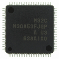
M30853FJGP#U3 Renesas Electronics America, M30853FJGP#U3 Datasheet - Page 529

M30853FJGP#U3
Manufacturer Part Number
M30853FJGP#U3
Description
IC M32C MCU FLASH 100LQFP
Manufacturer
Renesas Electronics America
Series
M16C™ M32C/80r
Datasheets
1.M3087BFLGPU3.pdf
(364 pages)
2.M30853FHFPD5.pdf
(94 pages)
3.M30853FHFPU3.pdf
(544 pages)
Specifications of M30853FJGP#U3
Core Processor
M32C/80
Core Size
16/32-Bit
Speed
32MHz
Connectivity
CAN, I²C, IEBus, SIO, UART/USART
Peripherals
DMA, WDT
Number Of I /o
85
Program Memory Size
512KB (512K x 8)
Program Memory Type
FLASH
Ram Size
24K x 8
Voltage - Supply (vcc/vdd)
3 V ~ 5.5 V
Data Converters
A/D 26x10b; D/A 2x8b
Oscillator Type
Internal
Operating Temperature
-40°C ~ 85°C
Package / Case
100-LQFP
For Use With
R0K330879S001BE - KIT DEV RSK M32C/87R0K330879S000BE - KIT DEV RSK M32C/87
Lead Free Status / RoHS Status
Lead free / RoHS Compliant
Eeprom Size
-
Available stocks
Company
Part Number
Manufacturer
Quantity
Price
Part Number:
M30853FJGP#U3M30853FJGP#D5
Manufacturer:
Renesas Electronics America
Quantity:
10 000
- Current page: 529 of 544
- Download datasheet (4Mb)
Rev.
REVISION HISTORY
Date
Page
299
301
302
303
304
308
310
350
356
360
364
379
381
382
383
388
389
390
391
392
393
• Figure 21.27 G1IRF Register and G0TB to G1TB Registers Note 2 of G1IRF
• Figure 21.29 CCS Register modified; Note 1 added
• 21.4.1 Clock Synchronous Serial I/O Mode (Communication units 0 and 1)
• Table 21.12 Clock Synchronous Serial I/O Mode Specifications (Communi-
• Table 21.14 Clock Settings (Communication Unit 1) Note 4 added
• Table 21.15 Registers to be Used and Settings Divided into Communication
• Table 21.16 Pin Settings in Clock Synchronous Serial I/O Mode (Communi-
• Figure 21.31 Transmit Operation modified
• Figure 21.32 Receive Operation modified
• Table 21.26 Clock Settings (Communication Unit 0) f
• Table 21.27 Clock Settings (Communication Unit 1) f
CAN Module
• Figure 22.31 C0SLOT0_4, C0SLOT1_4, C1SLOT0_4, and C1SLOT1_4
• 22.3.2.1 When the INTSEL Bit is Set to “0” modified
Programmable I/O Ports
• 23.9 Input Function Select Register (IPS and IPSA Registers)
• Figure 23.5 PD0 to PD15 Registers Note 4 revised
• Table 23.4 Port P7 Peripheral Function Output Control modified; Note 1
• Table 23.8 Port P11 Peripheral Function Output Control modified
• Table 23.9 Port P14 Peripheral Function Output Control modified
• Table 23.10 Port P15 Peripheral Function Output Control modified
Flash Memory Version
• Table 24.1 Flash Memory Version Specifications Note 3 added
• Figure 24.1 Flash Memory Block Diagram modified
• Figure 24.4 FMR0 and FMR1 Registers FMR1 register modified
• 24.3.3.1 FMR00 Bit Information added
• 24.3.3.3 FMR02 Bit revised
• Figure 24.5 How to Enter and Exit EW0 Mode Note 1 revised
• Figure 24.6 How to Enter and Exit EW1 Mode Note 2 revised
• Figure 24.7 Handling Before and After Low Power Consumption Mode
• 24.3.4.1 Operating Speed revised
register revised
revised
cation units 0 and 1) Note 1 deleted
Unit 1 and Communication Unit 2
cation Unit 0 and 1) (1) modified
Registers modified
added
Note 3 revised
M32C/85 Group(M32C/85, M32C/85T) Hardware Manual
C-10
Description
Summary
1
1
added
added
Related parts for M30853FJGP#U3
Image
Part Number
Description
Manufacturer
Datasheet
Request
R

Part Number:
Description:
KIT STARTER FOR M16C/29
Manufacturer:
Renesas Electronics America
Datasheet:

Part Number:
Description:
KIT STARTER FOR R8C/2D
Manufacturer:
Renesas Electronics America
Datasheet:

Part Number:
Description:
R0K33062P STARTER KIT
Manufacturer:
Renesas Electronics America
Datasheet:

Part Number:
Description:
KIT STARTER FOR R8C/23 E8A
Manufacturer:
Renesas Electronics America
Datasheet:

Part Number:
Description:
KIT STARTER FOR R8C/25
Manufacturer:
Renesas Electronics America
Datasheet:

Part Number:
Description:
KIT STARTER H8S2456 SHARPE DSPLY
Manufacturer:
Renesas Electronics America
Datasheet:

Part Number:
Description:
KIT STARTER FOR R8C38C
Manufacturer:
Renesas Electronics America
Datasheet:

Part Number:
Description:
KIT STARTER FOR R8C35C
Manufacturer:
Renesas Electronics America
Datasheet:

Part Number:
Description:
KIT STARTER FOR R8CL3AC+LCD APPS
Manufacturer:
Renesas Electronics America
Datasheet:

Part Number:
Description:
KIT STARTER FOR RX610
Manufacturer:
Renesas Electronics America
Datasheet:

Part Number:
Description:
KIT STARTER FOR R32C/118
Manufacturer:
Renesas Electronics America
Datasheet:

Part Number:
Description:
KIT DEV RSK-R8C/26-29
Manufacturer:
Renesas Electronics America
Datasheet:

Part Number:
Description:
KIT STARTER FOR SH7124
Manufacturer:
Renesas Electronics America
Datasheet:

Part Number:
Description:
KIT STARTER FOR H8SX/1622
Manufacturer:
Renesas Electronics America
Datasheet:

Part Number:
Description:
KIT DEV FOR SH7203
Manufacturer:
Renesas Electronics America
Datasheet:


