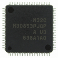
M30853FJGP#U3 Renesas Electronics America, M30853FJGP#U3 Datasheet - Page 533

M30853FJGP#U3
Manufacturer Part Number
M30853FJGP#U3
Description
IC M32C MCU FLASH 100LQFP
Manufacturer
Renesas Electronics America
Series
M16C™ M32C/80r
Datasheets
1.M3087BFLGPU3.pdf
(364 pages)
2.M30853FHFPD5.pdf
(94 pages)
3.M30853FHFPU3.pdf
(544 pages)
Specifications of M30853FJGP#U3
Core Processor
M32C/80
Core Size
16/32-Bit
Speed
32MHz
Connectivity
CAN, I²C, IEBus, SIO, UART/USART
Peripherals
DMA, WDT
Number Of I /o
85
Program Memory Size
512KB (512K x 8)
Program Memory Type
FLASH
Ram Size
24K x 8
Voltage - Supply (vcc/vdd)
3 V ~ 5.5 V
Data Converters
A/D 26x10b; D/A 2x8b
Oscillator Type
Internal
Operating Temperature
-40°C ~ 85°C
Package / Case
100-LQFP
For Use With
R0K330879S001BE - KIT DEV RSK M32C/87R0K330879S000BE - KIT DEV RSK M32C/87
Lead Free Status / RoHS Status
Lead free / RoHS Compliant
Eeprom Size
-
Available stocks
Company
Part Number
Manufacturer
Quantity
Price
Part Number:
M30853FJGP#U3M30853FJGP#D5
Manufacturer:
Renesas Electronics America
Quantity:
10 000
- Current page: 533 of 544
- Download datasheet (4Mb)
Rev.
REVISION HISTORY
Date
Page
101
102
105
107
109
115
117
118
119
120
120
129
130
135
136
145
151
152
153
80
85
87
90
93
94
97
99
Clock Generation Circuit
• Figure 9.1 Clock Generation Circuit Block diagram modified; f
• Figure 9.6 TCSPR and CPSRF Registers Note 2 added to the TCSPR register
• Figure 9.8 PM2 Register The PM24 and PM25 bits newly available
• Table 9.2 Bit Settings for On-Chip Oscillator Start Condition
• Table 9.4 CPU Clock Source and Bit Settings Main clock (main clock direct
• 9.3.4 f
• Table 9.6 BCLK/CLK
• Table 9.6 Pin States in Wait Mode Note 1 added
• 9.5.3 Stop Mode Interrupt usable to exit stop mode added; note 1 added
• Table 9.9 Pin Status in Stop Mode Note 1 added
• Figure 9.13 Status Transition in Wait Mode and Stop Mode Diagram modi-
• Figure 9.14 Status Transition Note 5 modified
Interrupts
• Figure 11.1 Interrupts Note 3 added
• 11.3.1.4 Low Voltage Detection Interrupt Note 1 added
• Table 11.1 Fixed Vector Table Note 1 added
• Figure 11.5 RLVL Register Value after reset changed
• 11.6.4 Interrupt Response Time Description modified
• Table 11.5 Interrupts without Interrupt Priority Levels and IPL Note1 added
• 11.6.6 Saving a Register Description modified; note 1 added
• Figure 11.8 Interrupt Priority Note 1 added
• Figure 11.9 Interrupt Priority Level Select Circuit Note 1 added
Watchdog Timer
• Figure 12.1 Watchdog Timer Block Diagram Diagram modified
• Figure 12.2 WDC Register and WDTS Register Note 3 added to the WDC register
DMAC
• Figure 13.2 DM0SL to DM3SLRegister Value after reset changed
• Table 13.2 DMiSL Register Function Note 3 modified
DMACII
• Figure 14.1 RLVL Register Value after reset changed; note 4 deleted
• 14.8 Execution Time Description modified
• Figure 14.5 Transfer Cycle The number of cycles changed
Timer
• Figure 15.1 Timer A Configuration Figure modified
• Figure 15.2 Timer B Configuration Figure modified
mode), the PM24 bit in the PM2 register and note 1 added
sor Mode Note 4 added
fied; note re-ordering due to previous note 2 deletion
CAN
M32C/85 Group(M32C/85, M32C/85T) Hardware Manual
Newly added
C-14
OUT
Pin in Memory Expansion Mode and Microproces-
Description
Summary
CAN
Newly added
added
Related parts for M30853FJGP#U3
Image
Part Number
Description
Manufacturer
Datasheet
Request
R

Part Number:
Description:
KIT STARTER FOR M16C/29
Manufacturer:
Renesas Electronics America
Datasheet:

Part Number:
Description:
KIT STARTER FOR R8C/2D
Manufacturer:
Renesas Electronics America
Datasheet:

Part Number:
Description:
R0K33062P STARTER KIT
Manufacturer:
Renesas Electronics America
Datasheet:

Part Number:
Description:
KIT STARTER FOR R8C/23 E8A
Manufacturer:
Renesas Electronics America
Datasheet:

Part Number:
Description:
KIT STARTER FOR R8C/25
Manufacturer:
Renesas Electronics America
Datasheet:

Part Number:
Description:
KIT STARTER H8S2456 SHARPE DSPLY
Manufacturer:
Renesas Electronics America
Datasheet:

Part Number:
Description:
KIT STARTER FOR R8C38C
Manufacturer:
Renesas Electronics America
Datasheet:

Part Number:
Description:
KIT STARTER FOR R8C35C
Manufacturer:
Renesas Electronics America
Datasheet:

Part Number:
Description:
KIT STARTER FOR R8CL3AC+LCD APPS
Manufacturer:
Renesas Electronics America
Datasheet:

Part Number:
Description:
KIT STARTER FOR RX610
Manufacturer:
Renesas Electronics America
Datasheet:

Part Number:
Description:
KIT STARTER FOR R32C/118
Manufacturer:
Renesas Electronics America
Datasheet:

Part Number:
Description:
KIT DEV RSK-R8C/26-29
Manufacturer:
Renesas Electronics America
Datasheet:

Part Number:
Description:
KIT STARTER FOR SH7124
Manufacturer:
Renesas Electronics America
Datasheet:

Part Number:
Description:
KIT STARTER FOR H8SX/1622
Manufacturer:
Renesas Electronics America
Datasheet:

Part Number:
Description:
KIT DEV FOR SH7203
Manufacturer:
Renesas Electronics America
Datasheet:


